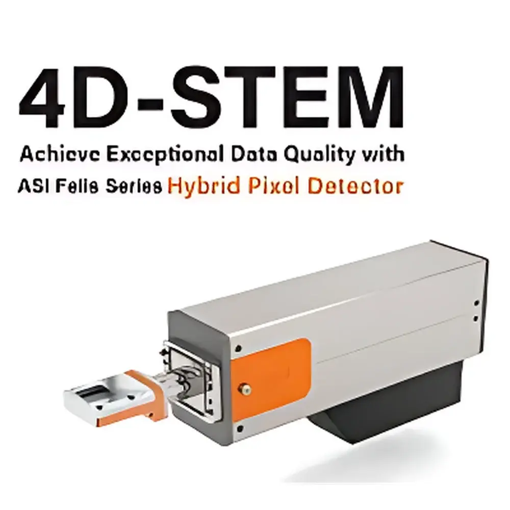
Amsterdam Scientific Instruments Felis T3 Hybrid Pixel Detector for 4D-STEM on SEM Platforms
| Brand | Amsterdam Scientific Instruments (ASI) |
|---|---|
| Origin | Netherlands |
| Model | Felis T3 |
| Acceleration Voltage Range | 0.5–30 kV |
| Sample Stage | 5-position 3 mm TEM grid holder |
| Detector Type | Hybrid pixel detector with nanosecond timestamping capability |
Overview
The Amsterdam Scientific Instruments Felis T3 is a high-performance hybrid pixel electron detector engineered specifically for scanning electron microscopy (SEM) platforms to enable quantitative 4D scanning transmission electron microscopy (4D-STEM). Unlike conventional scintillator- or CCD-based detectors, the Felis T3 operates in event-driven, time-stamped mode—capturing individual electron events with temporal resolution down to 1.56 ns. This architecture supports true data-driven acquisition, where each electron hit is recorded with precise spatial (x,y) and temporal (t) coordinates, forming a four-dimensional dataset: two real-space scan coordinates (x,y), one diffraction plane coordinate (qx,qy), and time-of-arrival metadata. When integrated into an SEM equipped with a thin specimen (e.g., electron-transparent 2D materials or lamellae prepared via FIB-SEM), the Felis T3 transforms the instrument into a versatile crystallographic analysis platform—capable of acquiring full 2D diffraction patterns at every probe position across a raster scan. This enables advanced structural characterization techniques traditionally restricted to dedicated TEM systems—including virtual imaging, differential phase contrast (DPC), ptychography, and transmission Kikuchi diffraction (TKD)—while leveraging the SEM’s inherent advantages in low-voltage operation, large field-of-view, and ease of sample handling.
Key Features
- Hybrid pixel sensor architecture with single-electron sensitivity and zero readout noise
- Nanosecond-scale timestamp resolution (1.56 ns binning) enabling time-resolved scattering analysis
- Event-driven acquisition mode eliminating frame-rate limitations and dead-time artifacts
- Native compatibility with standard SEM column geometries and vacuum interfaces (e.g., FEI/Thermo Fisher, Zeiss, JEOL)
- Optimized for low-acceleration-voltage operation (0.5–30 kV), enhancing elastic scattering cross-sections for light-element contrast
- Support for beam-sensitive specimen analysis via dose-controlled scanning and adaptive dwell time modulation
- Firmware-level support for synchronized trigger inputs (e.g., beam blanking, stage motion, external stimuli)
Sample Compatibility & Compliance
The Felis T3 is designed for use with electron-transparent specimens mounted on standard 3 mm TEM grids, compatible with widely adopted 5-position holders in modern SEM/FIB-SEM systems. It supports analysis of monolayer and few-layer 2D materials (graphene, h-BN, MoS₂, MXenes), Xenes (silicene, germanene), perovskites (including Ruddlesden–Popper phases), COFs, MOFs, and thin-film photovoltaic absorbers. All hardware and firmware comply with CE marking requirements for electromagnetic compatibility (EMC Directive 2014/30/EU) and low-voltage safety (LVD Directive 2014/35/EU). Data acquisition workflows are compatible with GLP-compliant environments when paired with audit-trail-enabled software frameworks such as LiberTEM or custom Python-based pipelines adhering to ISO/IEC 17025 traceability guidelines.
Software & Data Management
The Felis T3 integrates natively with open-source scientific computing ecosystems. Primary acquisition and real-time processing leverage the LiberTEM platform—a Python-based framework supporting HDF5-based 4D-STEM data storage (using the standardized “4D-STEM” NeXus extension). Raw event streams are written to lossless, chunked HDF5 files with embedded metadata (scan parameters, detector calibration, timestamp reference). Post-acquisition analysis includes center-of-mass (COM) DPC mapping, virtual detector synthesis (vLAADF, vMAADF, vHAADF), Bragg vector indexing, orientation mapping (via dictionary indexing or machine learning classifiers), and strain tensor reconstruction. All processing scripts are version-controlled and reproducible under POSIX-compliant HPC or workstation environments. Optional integration with commercial SEM control APIs (e.g., Thermo Fisher Avizo, Zeiss SmartSEM SDK) enables synchronized hardware triggering and metadata injection.
Applications
- Crystallographic orientation mapping at sub-10 nm spatial resolution using diffraction pattern indexing
- Phase identification and distribution mapping via angular correlation analysis of 4D datasets
- Local crystallinity and compositional gradient quantification through statistical analysis of Bragg peak intensities and widths
- Super-resolution ptychographic reconstruction from overlapping scan positions
- Differential phase contrast (DPC) imaging for electric/magnetic field visualization in functional oxides and heterostructures
- In-situ and operando studies under thermal, mechanical, or electrical bias using synchronized stimulus control
- Virtual annular detector imaging for multimodal contrast generation without physical reconfiguration
FAQ
What distinguishes Felis T3 from conventional SEM detectors?
The Felis T3 is not a secondary-electron or backscattered-electron detector—it is a direct-detection hybrid pixel sensor optimized for transmitted electrons in thin specimens, operating in event-mode with nanosecond timestamping.
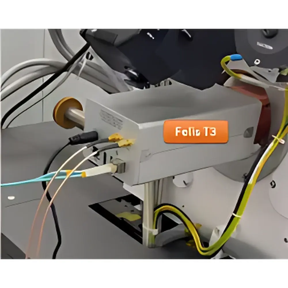
Can Felis T3 be installed on existing SEM systems?
Yes—mechanical and electrical integration kits are available for major SEM platforms (Thermo Fisher, Zeiss, JEOL); installation requires no modification to the column or vacuum system.
Is Felis T3 compatible with FIB-SEM dual-beam systems?
Yes—its compact form factor and low-voltage tolerance make it suitable for use in FIB-SEM configurations where lamella-based 4D-STEM is performed.
Does Felis T3 support FDA 21 CFR Part 11 compliance?
While the detector itself does not include built-in electronic signature or audit trail functionality, its HDF5 output format and integration with validated Python toolchains allow implementation of Part 11-compliant workflows in regulated environments.
What minimum specimen thickness is required for 4D-STEM with Felis T3?
Optimal performance is achieved with specimens <100 nm thick; monolayer 2D materials yield high-fidelity diffraction data even at 5–10 kV acceleration voltage.


