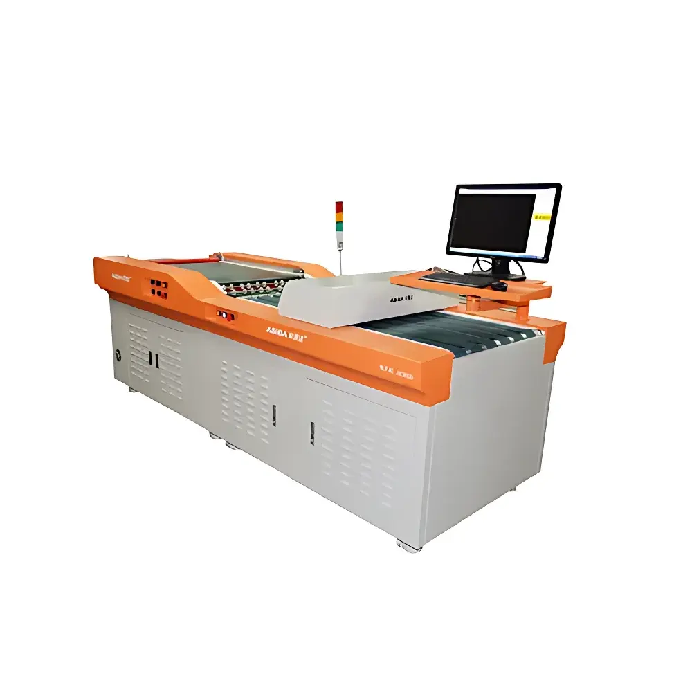
Asida JK3200 & JK3600 Automated PCB Via and Hole Inspection Systems
| Brand | Asida |
|---|---|
| Model | JK3200, JK3600 |
| Detectable Hole Diameter Range | 0.15–10 mm |
| PCB Size Range | 100 × 150 mm to 630 × 650 mm |
| PCB Thickness Range | 0.3–10 mm |
| Max. Hole Count per Board | 150,000 |
| Inspection Speed | 3.5–12.5 m/min (adjustable) |
| Hole Position Repeatability | ±40 µm |
| Hole Dimension Tolerance | ±40 µm |
| Minimum Hole-to-Hole Edge Distance | 0.15 mm |
| Detection Method | CIS Contact Image Sensor (Close-Range Linear Array Imaging) |
| Light Source | Diffuse Long-Strip LED Illumination |
| Power Supply | AC 220 V, 50 Hz |
| Compressed Air Requirement | 0.5–0.7 MPa |
| Dimensions (L×W×H) | 3550 × 1200 × 1100 mm |
| Weight | 450 kg |
| Origin | Guangdong, China |
| Distribution Type | Authorized Distributor |
Overview
The Asida JK3200 and JK3600 Automated PCB Via and Hole Inspection Systems are precision optical metrology platforms engineered for post-drilling quality assurance in printed circuit board (PCB) manufacturing. These systems employ high-resolution Contact Image Sensor (CIS) technology—mounted in close-proximity linear array configuration—to capture sub-pixel grayscale images of drilled vias, through-holes, and microvias across rigid, flex, and rigid-flex PCB substrates. Unlike traditional machine vision systems relying on telecentric lenses or CCD/CMOS area-scan cameras, the CIS-based architecture ensures consistent illumination geometry, minimal parallax error, and high spatial fidelity across large-format boards (up to 630 × 650 mm). The measurement principle is based on calibrated pixel-to-micron mapping, edge detection via adaptive thresholding, and sub-pixel centroid calculation—enabling traceable dimensional verification of hole diameter, positional deviation, plugging status (e.g., resin-filled, copper-capped, or open vias), and annular ring integrity. Designed for integration into final QA stations prior to packaging and shipment, both models comply with IPC-A-600 and IPC-6012 requirements for hole quality assessment and support statistical process control (SPC) data export for factory-wide quality management.
Key Features
- Dual- and hexa-board parallel inspection architecture: JK3200 supports simultaneous evaluation of two PCBs; JK3600 scales throughput with six independent conveyor lanes and synchronized CIS modules—each with dedicated real-time OK/NG classification logic.
- Zero-angle placement tolerance: Boards may be loaded within ±30° rotational deviation without recalibration, eliminating manual alignment and reducing cycle time by up to 35% versus fixed-orientation systems.
- Industrial-grade diffuse LED illumination: Long-life, spectrally stable linear LED arrays provide uniform, glare-free illumination across full board width—critical for consistent contrast in solder mask-covered or matte-finished substrates.
- Networked diagnostic station capability: Multiple client workstations can connect simultaneously to the host controller via Ethernet, enabling real-time remote viewing of NG defect maps—including false-color overlays of misaligned holes, undersized vias, or bridged pads—with timestamped audit logs.
- Field-upgradable firmware and inspection recipes: Parametric software architecture allows rapid deployment of new rule sets (e.g., custom hole size tolerances, multi-layer registration checks, or selective via inspection zones) without hardware modification or vendor dispatch.
Sample Compatibility & Compliance
The JK3200/JK3600 systems accommodate standard FR-4, high-Tg, polyimide, and metal-core PCBs with thicknesses from 0.3 mm to 10 mm—including multilayer boards with blind/buried vias. Support extends to panelized arrays (depanelized or tab-routed) and single-board formats. All image acquisition, defect classification, and reporting functions adhere to ISO/IEC 17025 calibration traceability principles. System-generated inspection reports include metadata compliant with IPC-D-356A netlist alignment validation and support GLP/GMP-aligned electronic record retention when integrated with validated LIMS or MES platforms. Optional 21 CFR Part 11-compliant user authentication and electronic signature modules are available for regulated medical device PCB production environments.
Software & Data Management
The proprietary Asida VisionInsight™ software suite provides a unified interface for recipe creation, real-time dashboard monitoring, SPC charting (X-bar/R, Cpk), and root-cause analysis. Each inspection generates a structured XML report containing raw coordinate data, pass/fail status per hole, confidence scores, and annotated defect thumbnails. Data export supports CSV, JSON, and OPC UA protocols for seamless integration with factory automation systems. Audit trails record all operator actions, parameter changes, and system events with SHA-256 hashing—ensuring full accountability during internal or third-party quality audits. Software updates are delivered via secure HTTPS channel with cryptographic signature verification.
Applications
- Final QA verification of drilled via count, diameter, and positional accuracy prior to electroplating or solder mask application.
- Automated detection of common defects: missing holes, oversized/undersized vias, misdrilled locations, resin smearing, copper burrs, and partial plugging.
- High-volume inspection of small-form-factor PCBs (e.g., smartphone modules, wearables, IoT sensors) where JK3600’s six-lane throughput achieves >120 boards/hour at 630 × 650 mm max size.
- Process capability studies for drilling equipment maintenance scheduling—correlating hole size drift with drill bit wear cycles.
- Supplier qualification and incoming material inspection for contract manufacturers requiring documented evidence of IPC Class 2 or Class 3 conformance.
FAQ
What standards does this system reference for hole measurement accuracy?
The system’s dimensional calibration follows ISO 10360-2 (coordinate measuring machines) and NIST-traceable step gauges. Hole diameter uncertainty is validated per ISO/IEC 17025 Annex A.5 using certified aperture standards.
Can the system inspect laser-drilled microvias (<100 µm)?
No. The minimum detectable hole diameter is 0.15 mm (150 µm); microvia inspection requires scanning electron microscopy (SEM) or specialized laser confocal systems.
Is offline programming supported for custom board layouts?
Yes—Gerber RS-274X and ODB++ import enables automatic fiducial recognition and region-of-interest definition without physical board loading.
Does the system support AOI-style solder joint inspection?
No. This platform is purpose-built for mechanical hole metrology only; solder joint analysis requires dedicated automated optical inspection (AOI) hardware with angled lighting and 3D height profiling.
What maintenance intervals are recommended for the CIS modules?
CIS sensor cleaning is advised every 200 operating hours; LED light source lifetime exceeds 20,000 hours under continuous operation—verified via built-in photometric monitoring.


")
