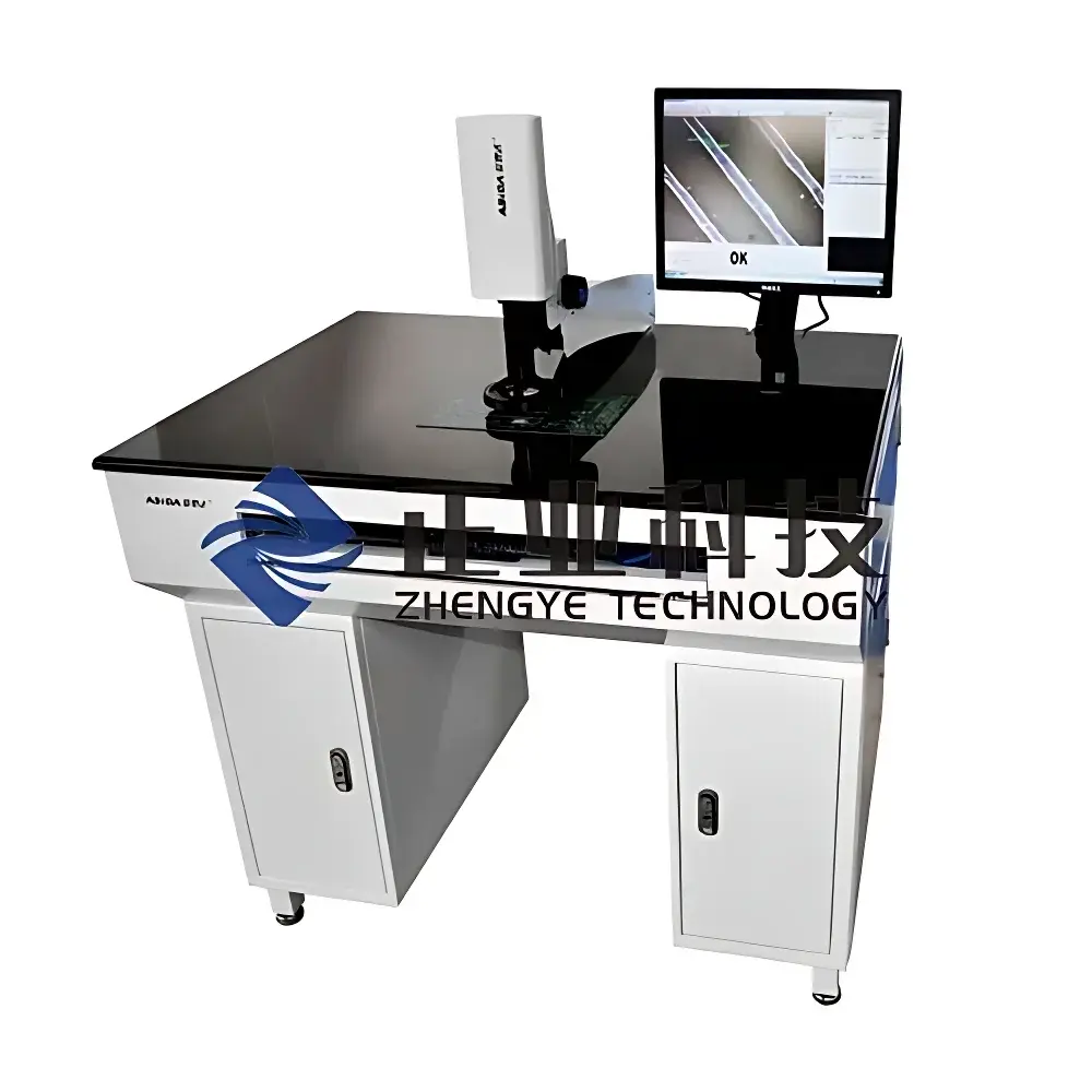
ASIDA XK22 PCB Trace Width Measurement System
| Brand | ASIDA |
|---|---|
| Model | XK22 |
| Origin | Guangdong, China |
| Type | Optical Metrology System for Printed Circuit Board Inspection |
| Measurement Principle | High-Resolution Digital Microscopy with Sub-Pixel Edge Detection |
| Max. Board Width | ≤760 mm |
| Field of View | 0.53×0.4 mm to 3.4×2.5 mm |
| Minimum Measurable Line Width | ≥20 µm |
| Measurement Accuracy | ±1 µm |
| Pixel Resolution | 0.70–5.20 µm/pixel |
| Total Magnification Range | 70×–450× |
| Optical Zoom | 1.4×–9× Continuous |
| SPC Capability | Yes |
| Illumination | Red LED Targeting Light |
| Weight (system only) | 145 kg |
| Dimensions (W×D×H, excl. PC) | 960×700×1280 mm |
| Compliance | Designed for IPC-6012, IPC-A-600, and ISO 9001-aligned QA/QC workflows |
| Software | Proprietary ASIDA Vision Suite with Audit Trail & Export to CSV/XLSX |
Overview
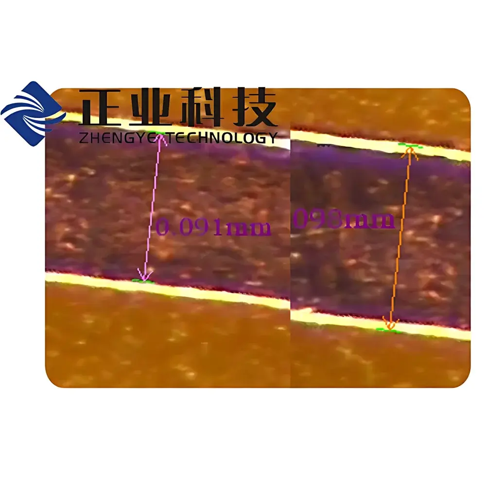
The ASIDA XK22 PCB Trace Width Measurement System is a precision optical metrology platform engineered for non-contact, high-repeatability dimensional analysis of printed circuit board (PCB) features during mid- and post-etch fabrication stages. It operates on the principle of high-magnification digital microscopy combined with sub-pixel edge localization algorithms—leveraging calibrated optics, stable mechanical staging, and deterministic image processing to quantify critical dimensions including trace width (top and bottom), trace-to-trace spacing, pad-to-trace clearance, via-to-edge distance, circular/oval hole diameters, and curved feature radii. Designed specifically for use prior to solder mask application, the system supports both rigid PCBs and flexible printed circuits (FPCs), as well as auxiliary applications in semiconductor wafer bump inspection, thin-film electrode patterning, and LCD panel conductor metrology. Its architecture conforms to foundational requirements of IPC-6012 Class 2 and Class 3 verification protocols, enabling traceable measurement data suitable for internal process control and supplier qualification audits.
Key Features
- Sub-pixel edge detection engine delivering measurement repeatability within ±1 µm across repeated acquisitions under controlled environmental conditions.
- Motorized continuous optical zoom (1.4×–9×) paired with fixed-focus telecentric objectives to maintain depth-of-field stability across magnification ranges; total system magnification spans 70× to 450×.
- Red LED targeting illumination for rapid visual alignment and operator-assisted positioning—minimizing setup time without compromising photometric consistency.
- Automated edge recognition with adaptive thresholding and noise-resistant contour interpolation, optimized for low-contrast copper traces on etched substrates.
- Integrated Statistical Process Control (SPC) module supporting real-time X-bar/R chart generation, Cp/Cpk calculation, and out-of-control condition flagging per ANSI/ASQ B18.1 standards.
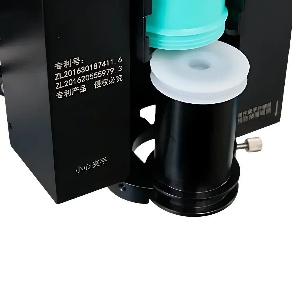
- Rigid granite-base mechanical structure with vibration-damped isolation feet; designed to sustain metrological integrity in shared factory-floor environments.
Sample Compatibility & Compliance
The XK22 accommodates PCB panels up to 760 mm in width and supports automated XY stage traversal across defined inspection zones. Its field-of-view range (0.53×0.4 mm to 3.4×2.5 mm) enables both localized high-resolution interrogation and broader pattern sampling. The system is validated for measurements on copper-clad FR-4, polyimide-based FPCs, silicon wafers with metalized interconnects, and ITO-patterned glass substrates. All measurement workflows are structured to align with IPC-A-600G acceptability criteria for conductor geometry, and raw coordinate data can be exported with timestamped metadata to satisfy internal GLP documentation or external ISO 9001 clause 7.1.5 audit requirements. While not FDA 21 CFR Part 11-certified out-of-the-box, the ASIDA Vision Suite supports configurable user access levels and optional electronic signature modules for regulated environments.
Software & Data Management
The ASIDA Vision Suite provides a Windows-based interface with dual operational modes: manual single-point measurement and batch-mode automated grid scanning. Each measurement record includes image capture (TIFF/PNG), pixel-coordinate mapping, calibrated physical dimension output (µm/mm), statistical summaries, and SPC chart overlays. Data export options include CSV, XLSX, and XML formats compatible with MES integration layers. Audit trail functionality logs all user actions—including parameter modifications, calibration events, and report generation—with immutable timestamps. Calibration certificates (traceable to NIST-traceable reference standards) are stored alongside instrument configuration profiles and may be regenerated following scheduled recalibration intervals recommended by ASIDA’s service protocol.
Applications
- Final verification of inner/outer layer etch performance pre-solder mask application.
- Process capability assessment of fine-line (<50 µm) and HDI microvia architectures.
- Root cause analysis of undercutting, over-etching, or sidewall taper anomalies via comparative top/bottom width ratio reporting.
- Qualification of photolithography tool performance across multiple exposure lots.
- Supplier incoming inspection for multilayer stack-up dimensional conformance.
- Research-grade line-width uniformity mapping for advanced packaging substrates and embedded passive structures.
FAQ
What is the minimum measurable line width supported by the XK22?
The system is validated for reliable measurement of conductive traces ≥20 µm in nominal width under standard lighting and focus conditions.
Does the XK22 support automatic pass/fail judgment against user-defined tolerances?
Yes—tolerance bands can be assigned per feature type (e.g., line width, spacing), with visual highlighting and CSV log flags generated for deviations.
Is the optical path calibrated for thermal drift compensation?
No active thermal compensation is implemented; however, the system achieves <±0.3 µm thermal drift over 2-hour stabilization at 23±1°C ambient per ISO 230-3 guidelines.
Can measurement data be integrated into a central MES or QMS platform?
Yes—via standardized file export or optional OPC UA interface add-on for real-time data streaming to enterprise quality databases.
What maintenance schedule does ASIDA recommend for long-term accuracy retention?
Quarterly verification using certified step gauges and annual full recalibration by ASIDA-certified service engineers are advised.