Atometrics AF-3000 Series T010 Thin-Film Thickness Metrology System
| Brand | Atometrics |
|---|---|
| Origin | Guangdong, China |
| Manufacturer Type | Original Equipment Manufacturer (OEM) |
| Product Origin | Domestic (China) |
| Model | AF-3000 Series T010 |
| Pricing | Available Upon Request |
Overview
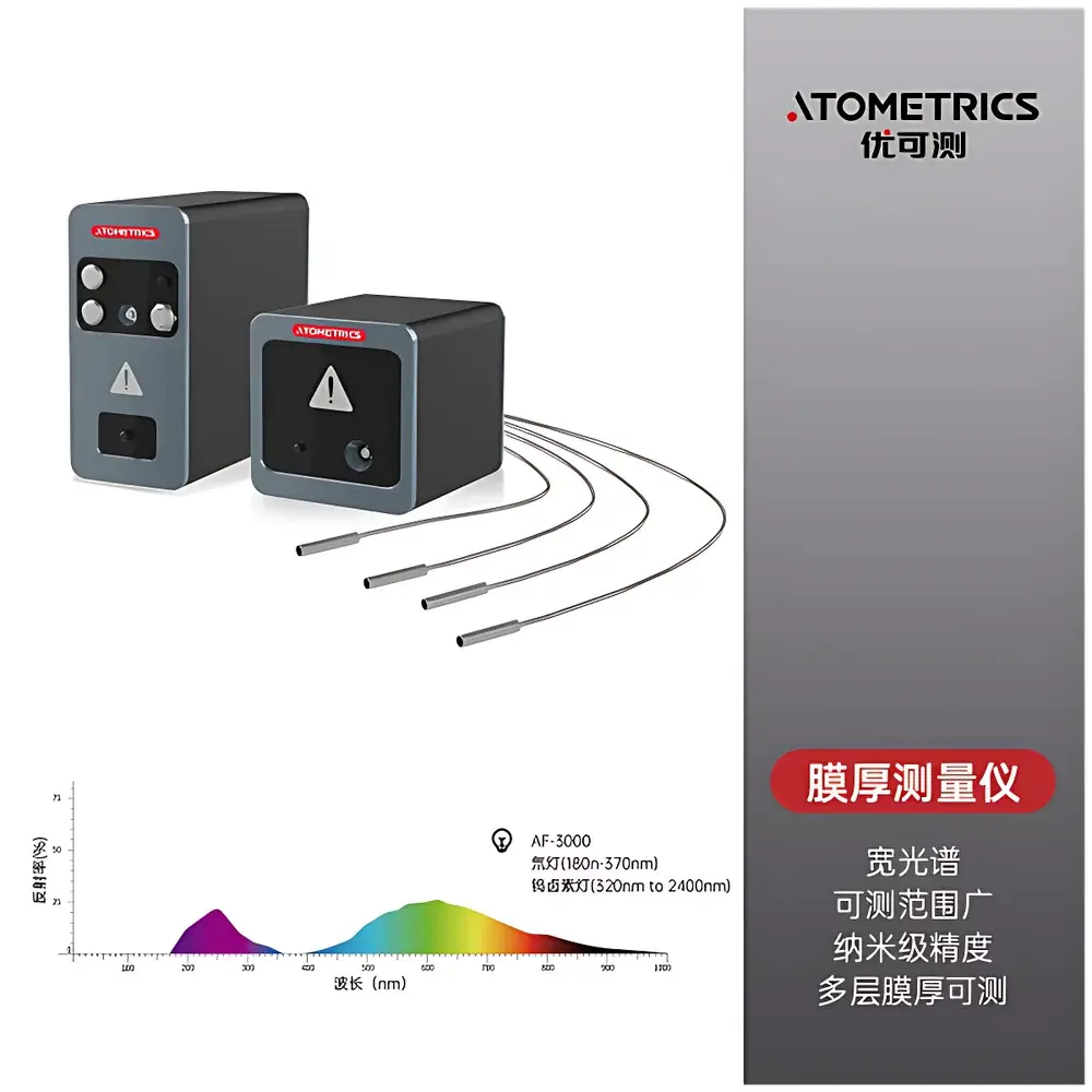
The Atometrics AF-3000 Series T010 is a high-precision, non-contact optical thin-film thickness metrology system engineered for nanoscale dimensional characterization of single- and multi-layer dielectric, semiconductor, and polymer films. It operates on the principle of spectral reflectometry—measuring wavelength-dependent reflectance across the deep ultraviolet to near-infrared spectrum (180–2400 nm) and reconstructing film thickness and optical constants via rigorous physical modeling of interference fringes. Unlike conventional broadband reflectometers relying on global curve fitting, the AF-3000 T010 implements a proprietary segmented spectral fitting algorithm that partitions the spectrum into physically meaningful sub-bands (e.g., UV, visible, NIR), independently optimizing layer parameters within each region. This approach significantly reduces parameter correlation and systematic bias—particularly critical for complex stacks containing ITO, perovskite, quantum dots, SiO₂, PI, photoresist, or bonded glass wafers—thereby achieving sub-angstrom (≤0.1 nm) thickness resolution under controlled calibration conditions.
Key Features
- Multi-source illumination architecture: Deuterium lamp (180–370 nm) + tungsten-halogen lamp (320–2400 nm), delivering stable, uniform spectral irradiance with minimal drift over extended measurement cycles
- Segmented spectral fitting engine: Dynamically partitions reflectance data into domain-specific bands, enabling robust convergence for up to 10-layer stack models—even with rough interfaces or dispersive materials
- High-speed acquisition: Sub-100 ms per spectrum, supporting real-time process monitoring in inline and at-line configurations
- Flexible deployment modes: Benchtop offline unit, compact inline module (<150 mm footprint), and fully automated wafer-handling integration for 4″–12″ substrates
- Sub-Ångström resolution capability: Achieved through optimized optical path design, thermal stabilization, and advanced noise suppression in detector electronics
- Material-agnostic modeling: Supports Cauchy, Sellmeier, Tauc-Lorentz, and user-defined dispersion models for accurate n(λ) and k(λ) reconstruction
Sample Compatibility & Compliance
The AF-3000 T010 accommodates a broad range of substrate geometries and surface conditions—including flat wafers, curved optics, flexible foils, and microfluidic channels—with no requirement for vacuum or sample coating. It measures transparent, semi-transparent, and weakly absorbing films on silicon, glass, sapphire, metal, and polymer substrates. Surface roughness up to 5 nm RMS does not compromise measurement fidelity due to integrated scatter correction in the optical model. The system complies with ISO/IEC 17025 calibration traceability requirements when operated with NIST-traceable reference standards. Measurement workflows support audit-ready documentation aligned with GLP and GMP environments; raw spectra, fit residuals, and parameter covariance matrices are stored with full metadata (timestamp, operator ID, instrument configuration) to satisfy FDA 21 CFR Part 11 electronic record integrity requirements.
Software & Data Management
Control and analysis are performed via Atometrics’ MetroSuite v4.x software—a Windows-based application featuring modular workflow scripting, batch processing, and SPC dashboarding. All optical models are editable in XML format, allowing users to define custom layer sequences, interface roughness profiles, and dispersion relations. Measurement reports export to CSV, PDF, and HDF5 formats, with optional integration into factory MES systems via OPC UA or RESTful API. Audit trails log every parameter change, fit iteration, and report generation event. Software validation packages—including IQ/OQ documentation, test protocols, and UAT checklists—are available for regulated industries.
Applications
- Process development and control of ALD, PVD, and spin-coated layers in display and photovoltaic manufacturing (e.g., ITO, perovskite, QD emissive layers)
- In-line thickness verification during anti-reflective coating deposition on precision optics and camera lenses
- Quality assurance of PI and polyimide films used in flexible PCBs and foldable display backplanes
- R&D metrology for multilayer barrier stacks in OLED encapsulation and micro-LED transfer processes
- Characterization of sol-gel derived SiO₂ and Al₂O₃ films for MEMS passivation and sensor functionalization
- Thickness mapping across 300 mm wafers using motorized X-Y stages (optional)
FAQ
What is the minimum measurable thickness for a single SiO₂ layer on silicon?
For thermally grown SiO₂ on silicon, the practical lower limit is ~0.8 nm with ≤0.05 nm repeatability (3σ) under optimized signal-to-noise conditions.
Can the system measure films on highly curved substrates?
Yes—curvature radii down to 5 mm are supported via adjustable focus optics and custom beam-shaping apertures; measurement uncertainty increases by <±0.3 nm per 1 mm radius reduction beyond 10 mm.
Is ASTM E2375-22 compliance supported?
MetroSuite includes preconfigured templates and uncertainty budgets compliant with ASTM E2375-22 for optical thickness measurement of transparent films; full compliance requires site-specific validation using certified reference materials.
How is calibration maintained across lamp aging?
The system performs daily auto-calibration using an internal reference mirror and embedded photodiode array; spectral stability is tracked via built-in deuterium line monitoring at 241.8 nm and 361.0 nm.
Does the software support custom scripting for automated recipe switching?
Yes—Python 3.9 runtime is embedded; users may define conditional logic for auto-selecting models, wavelengths, and fit constraints based on barcode-scanned lot IDs or sensor inputs.


")
