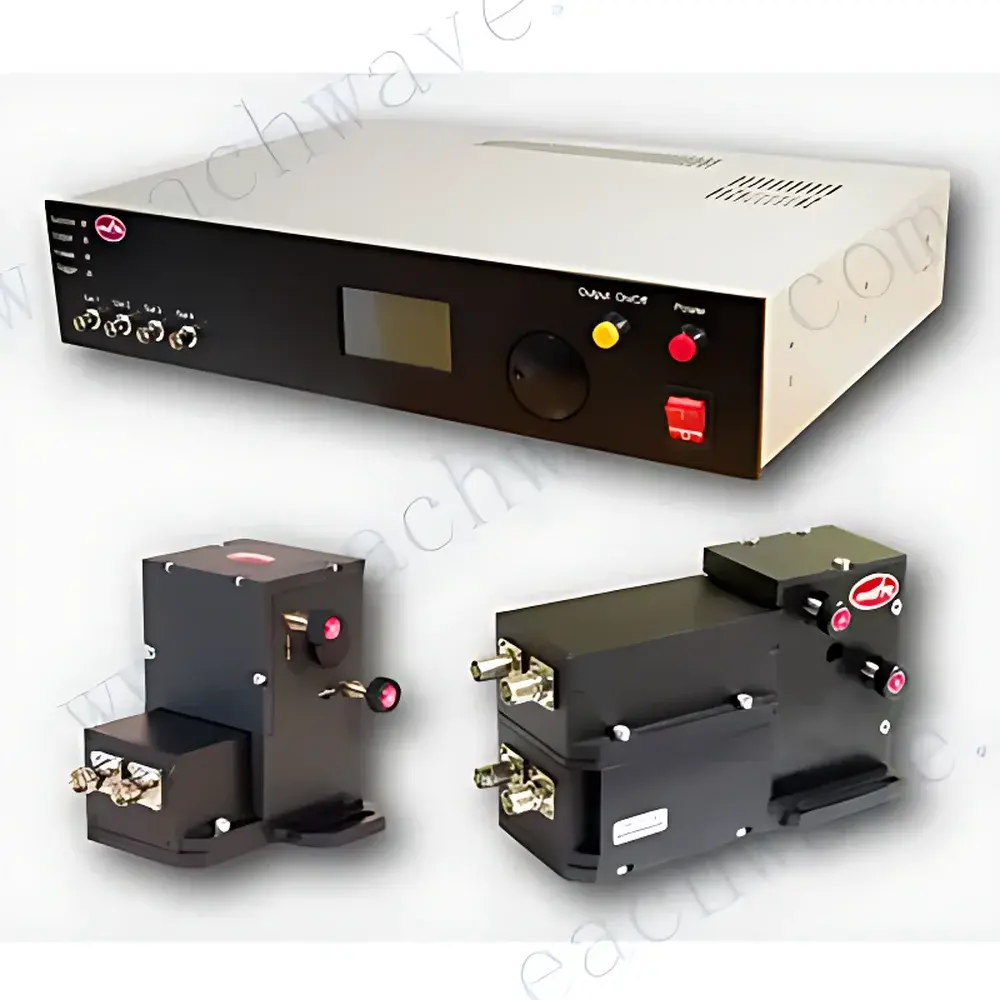
ATSEVA OG-B/F Series Electro-Optic Pulse Pickers for Ultrafast Lasers
| Brand | ATSEVA |
|---|---|
| Origin | Russia |
| Model | OG-B/F |
| Core Components | Pockels Cell, High-Voltage Gate Driver, Synchronization & Delay Module |
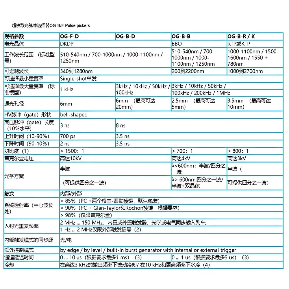
| Wavelength Ranges | 340–1280 nm (OG-F), 200–2200 nm (OG-B), 1000–2700 nm (OG-B-R/K) |
| Max Repetition Rate | 1 MHz (OG-B-R/K), 100 kHz (OG-B), 1 kHz (OG-F) |
| Minimum Repetition Rate | Single-shot |
| Aperture | Up to 20 mm (OG-B), 6 mm (OG-F), 3.5 mm (OG-B-R/K) |
| HV Gate Pulse Width (10% level) | 3 ns (OG-F), 8 ns (OG-B), 8 ns (OG-B-R/K) |
| Rise Time (10–90%) | 700 ps (OG-F), 3.5 ns (OG-B/OG-B-R/K) |
| Contrast Ratio | >1500:1 (OG-F), >700:1 (OG-B), >800:1 (OG-B-R/K) |
| Pockels Cell Voltage | up to 10 kV (OG-F), up to 4 kV (OG-B), up to 3 kV (OG-B-R/K) |
| Transmission | >85% (standard GT prism + PC), >98% (PC only) |
| Trigger Options | Internal/External, Optical/Electrical, Edge/Level/Burst Mode |
| Channel Delay Range | 0–10 µs (OG-F), 0–1 µs (OG-B/OG-B-R/K), extendable per request |
| Cooling | Passive ≤3 kHz |
Overview
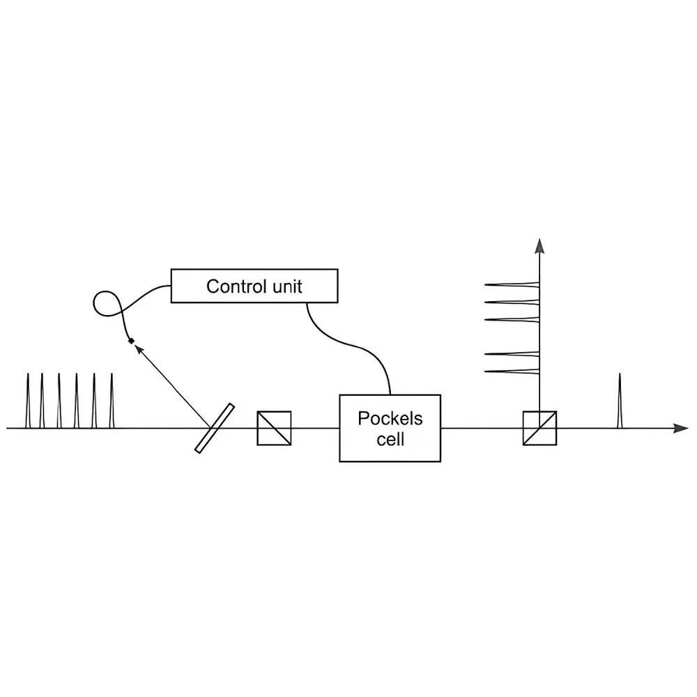
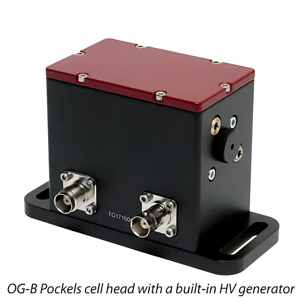
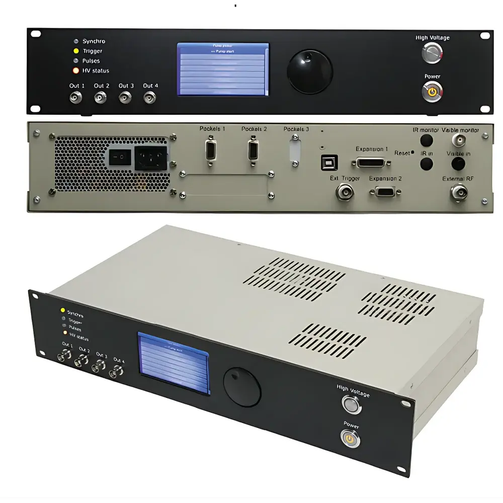
The ATSEVA OG-B/F Series Electro-Optic Pulse Pickers are precision timing and amplitude control instruments engineered for deterministic selection of individual pulses from high-repetition-rate ultrafast laser trains. Based on the Pockels effect in nonlinear electro-optic crystals—such as DKDP, BBO, RTP, or KTP—these systems operate as synchronized optical switches, enabling gated transmission with sub-nanosecond temporal resolution. The OG-F variant is optimized for visible-to-NIR femtosecond sources (e.g., Ti:sapphire oscillators at 800 nm), while the OG-B and OG-B-R/K models support broader spectral coverage—from UV (200 nm) through mid-IR (2700 nm)—making them suitable for Yb-, Er-, Tm-, and Cr:ZnSe-based amplifier systems. Each unit integrates a low-jitter high-voltage pulse generator, a thermally stabilized crystal mount, and a modular synchronization interface, ensuring phase-locked operation with input pulse trains ranging from 1 Hz to 150 MHz.
Key Features
- Sub-ns gate timing fidelity: 700 ps rise time (OG-F), <2 ns full-width-at-10%-level (OG-F), enabling clean isolation of adjacent femtosecond pulses without temporal broadening.
- High extinction contrast: >1500:1 (OG-F), >700:1 (OG-B), >800:1 (OG-B-R/K), defined as the ratio of selected-pulse energy to residual energy in adjacent time slots—critical for amplifier seed injection and pre-pulse suppression.
- Flexible triggering architecture: Supports internal optical/electrical sync, external TTL/LVDS inputs, edge- or level-sensitive gating, and built-in burst generation with programmable pulse count and inter-burst delay.
- Configurable optical layout: Standard configuration includes Pockels cell + two Glan-Taylor prisms (>85% system transmission); optional Rochon-prism integration achieves >90% transmission; bare-cell mode delivers >98% throughput for integration into custom beamlines.
- Scalable thermal management: Passive cooling suffices up to 3 kHz output rate; water-cooling (1 L/min, 20–22°C) enables stable operation at 100 kHz–1 MHz, with total dissipated heat limited to <80 W (excluding chiller).
- LabVIEW-compatible USB 2.0 interface with SCPI command set, supporting remote parameter adjustment (delay, gate width, trigger mode) and real-time status monitoring (HV temperature, sync lock, pulse detection).
Sample Compatibility & Compliance
The OG-B/F series accommodates free-space Gaussian beams with M² < 1.3 and divergence < 1 mrad. Input polarization must be linear and aligned to the crystal’s principal axis; optional half-wave plates enable rotation for arbitrary input SOP. All models comply with IEC 61000-6-3 (EMC emission) and IEC 61010-1 (safety for laboratory equipment). For regulated environments, firmware supports audit-trail logging (timestamped parameter changes) and user-access-level controls—aligning with GLP/GMP documentation requirements. While not FDA 21 CFR Part 11 certified out-of-the-box, the LabVIEW API permits integration with validated data acquisition frameworks meeting Part 11 electronic record criteria.
Software & Data Management
Control is implemented via a vendor-provided LabVIEW VI suite, offering intuitive front panels for delay calibration, HV pulse profiling, and jitter measurement using integrated photodiode feedback. Raw timing data (trigger latency, gate jitter, pulse-to-pulse delay stability) can be exported in CSV or HDF5 format. The SCPI command layer enables seamless integration with Python (PyVISA), MATLAB, or EPICS-based control systems. Firmware updates are delivered via signed binary packages with SHA-256 verification. Configuration files store device-specific calibration coefficients—including wavelength-dependent half-wave voltage (Vλ) and thermal drift compensation curves—for automated compensation across operating conditions.
Applications
- Regenerative amplifier seeding: Selecting single pulses from MHz oscillator outputs to match amplifier cavity round-trip time, minimizing gain depletion and ASE buildup.
- Contrast enhancement in CPA systems: Removing pre-pulses and post-pulses preceding the main amplified pulse—improving temporal contrast by >3 orders of magnitude before compressor stages.
- Time-resolved pump-probe spectroscopy: Generating precisely timed probe pulses with adjustable delay relative to pump, enabling fs-resolution dynamics studies in condensed matter and molecular physics.
- Ultrafast metrology: Pulse train decimation for autocorrelator or FROG characterization where detector bandwidth limits direct measurement.
- Quantum optics experiments: On-demand photon-pair generation gating in SPDC sources, synchronized to single-photon detector dead time.
FAQ
What is the minimum input repetition rate supported in internal trigger mode?
Internal triggering requires a minimum input pulse train frequency of 2 MHz to maintain stable synchronization; for lower rates (1 Hz–2 MHz), external electrical or optical triggering is mandatory.
Can the OG-B/F be used with amplified femtosecond pulses exceeding 1 mJ?
Yes—provided peak fluence remains below 0.5 J/cm² at the Pockels cell aperture and average power does not exceed the crystal’s thermal lensing threshold (typically <5 W for DKDP, <10 W for BBO). Optional AR-coated crystals and enlarged apertures (up to 20 mm) are available for high-energy applications.
Is wavelength tuning possible without hardware modification?
No—each model is calibrated for specific wavelength bands. However, custom configurations (e.g., dual-crystal stacks for broadband operation or waveplate-integrated mounts for polarization agility) can be ordered as OEM variants.
How is timing jitter quantified and minimized?
Jitter is measured as RMS deviation of gate onset relative to sync input, typically <200 ps (OG-F) and <350 ps (OG-B/OG-B-R/K) under optimal conditions. Minimization relies on low-inductance HV cabling, impedance-matched trigger paths, and temperature-stabilized crystal mounts.
Does the system support multi-channel parallel pulse selection?
Not natively—the OG-B/F is a single-channel device. However, multiple units can be synchronized via common master clock and distributed delay lines for multi-beam or multi-wavelength selection schemes, with inter-unit skew <100 ps when using optical sync distribution.


