Attension Theta Wafer Video Optical Contact Angle Analyzer for Semiconductor Wafers
| Brand | Attension |
|---|---|
| Origin | Finland |
| Model | Theta Wafer |
| Instrument Type | Benchtop Video Optical Contact Angle Analyzer |
| Measurement Capabilities | Contact Angle, Surface Tension, Interfacial Tension, Surface Free Energy |
| Contact Angle Accuracy | ±0.1° |
| Contact Angle Resolution | 2592 × 2048 (5 MP) |
| Maximum Sample Size | 12-inch wafer |
| Sample Stage Load Capacity | 500 g |
| Rotational Range | 0–360° |
| Maximum Rotation Speed | 180°/s |
| Angular Resolution | 0.005° |
| Vacuum Interface | Yes |
| Automated Positioning | Yes |
| Camera Frame Rate | Up to 3422 fps |
Overview
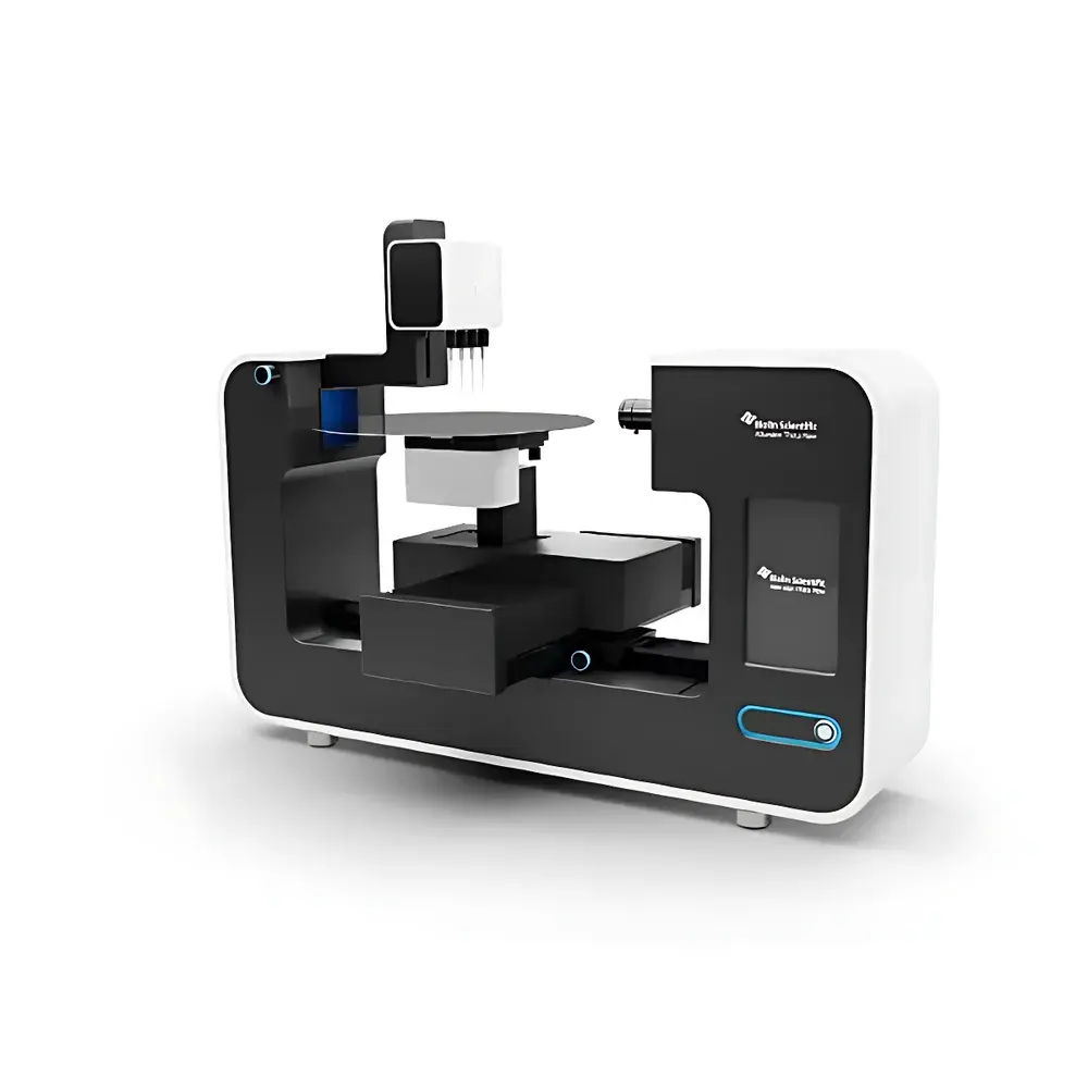
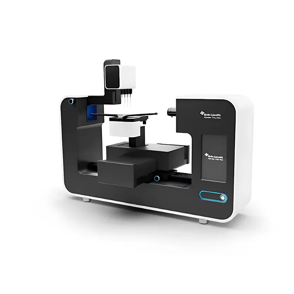
The Attension Theta Wafer is a purpose-engineered benchtop video optical contact angle analyzer designed exclusively for high-precision surface characterization of semiconductor wafers up to 300 mm (12 inches) in diameter. It operates on the principle of sessile drop analysis using high-resolution digital imaging and advanced edge-detection algorithms to quantify the contact angle formed between a precisely dispensed liquid droplet and the solid wafer surface. This measurement serves as a direct indicator of surface wettability, interfacial energetics, and chemical homogeneity—parameters critical to photolithography, thin-film deposition, wafer bonding, and cleaning process validation. Unlike general-purpose contact angle systems, the Theta Wafer integrates a motorized, software-controlled rotational stage with XYZ translation and vacuum-assisted wafer clamping, enabling fully automated, repeatable positioning across the entire wafer surface. Its optical architecture supports both static and dynamic contact angle measurements—including advancing/receding angles—and facilitates quantitative derivation of surface free energy via multi-liquid methods (e.g., Owens-Wendt, Wu, or van Oss approaches). The system complies with fundamental metrological requirements outlined in ASTM D7334 (Standard Practice for Surface Wettability of Polymer Coatings) and ISO 19403 (Contact angle measurement by optical tensiometry), ensuring traceable, laboratory-grade data suitable for process development and quality assurance workflows.
Key Features
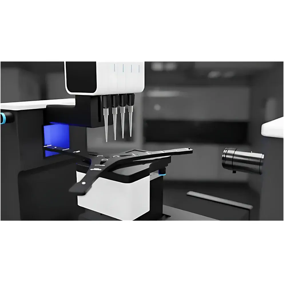
- Fully automated, software-synchronized XYZ translation stage with motorized 360° rotation (T340R + T340RW wafer chuck), enabling precise radial and angular positioning across 2″ to 12″ wafers.
- Vacuum-compatible wafer holder with precision alignment pins and integrated vacuum port for secure, vibration-free immobilization during measurement.
- High-speed CMOS camera (5 MP resolution, 2592 × 2048 pixels) capable of capturing up to 3422 frames per second—essential for dynamic contact angle analysis and droplet oscillation studies.
- Optional quad-channel automated dispensing system with four software-controlled, disposable pipette tips, supporting sequential multi-liquid surface free energy mapping without cross-contamination.
- Angular resolution of 0.005° and contact angle repeatability better than ±0.1°, validated under controlled environmental conditions (temperature-stabilized lab environment, ISO Class 7 cleanroom compatible).
- Benchtop footprint optimized for integration into semiconductor R&D labs and pilot-line process control environments.
Sample Compatibility & Compliance
The Theta Wafer accommodates standard silicon, SOI, GaN, SiC, and glass wafers ranging from 50.8 mm (2″) to 300 mm (12″) in diameter, with maximum load capacity of 500 g. Its modular stage design allows rapid reconfiguration for alternative substrates including patterned wafers, MEMS devices, and temporary bonding carriers. All hardware and firmware components are engineered to meet CE marking requirements and comply with IEC 61000-6-3 (EMC emissions) and IEC 61000-6-2 (immunity). Data acquisition and storage protocols support audit trails required under GLP and GMP frameworks; optional software modules provide 21 CFR Part 11-compliant electronic signatures and user-access logging for regulated environments.
Software & Data Management
Theta Suite software provides a unified interface for instrument control, image acquisition, real-time contact angle calculation, and statistical reporting. Batch measurement mode enables unattended sequential analysis across multiple wafers or predefined grid positions—ideal for process qualification and lot acceptance testing. Built-in analysis tools include baseline correction algorithms for non-horizontal surfaces, tangent and circle fitting options, and automatic droplet volume calibration. Export formats include CSV, PDF, and XML, with metadata tagging for sample ID, operator, timestamp, environmental conditions (optional humidity/temperature sensor input), and measurement method. Raw image sequences and processed data sets are stored in a structured local database with version-controlled backups and configurable retention policies.
Applications
- Process validation of wafer cleaning efficacy—quantifying residual hydrophobic contaminants via increased contact angle after RCA or plasma treatment.
- Surface energy mapping of spin-coated photoresists to correlate contact angle hysteresis with film uniformity and crosslink density.
- Adhesion assessment of dielectric layers (e.g., SiO₂, SiNₓ) prior to metallization or bonding, where low surface energy correlates with poor metal adhesion.
- Hydrophilicity/hydrophobicity profiling of ALD-grown functional coatings used in microfluidic or biosensor applications.
- In-process QC monitoring during wafer-level packaging—detecting surface contamination or oxidation-induced wettability shifts before underfill dispensing.
FAQ
What wafer sizes does the Theta Wafer support?
The system supports standard diameters from 2″ (50.8 mm) to 12″ (300 mm), with interchangeable chucks and alignment fixtures for each size.
Can the Theta Wafer measure dynamic contact angles?
Yes—its high-speed camera (up to 3422 fps) and synchronized dispensing enable advancing/receding angle measurement, roll-off analysis, and evaporation kinetics studies.
Is surface free energy calculation automated?
Yes—Theta Suite includes built-in models (Owens-Wendt, Wu, van Oss) and supports user-defined liquid libraries; multi-liquid measurements can be executed automatically using the optional quad-dropper module.
Does the system require external vacuum supply?
Yes—a standard industrial vacuum source (−80 kPa minimum) connects via the integrated port to secure wafers during rotation and translation.
How is measurement traceability ensured?
All contact angle values are derived from pixel-registered image analysis with geometric calibration using certified reference standards; system performance verification reports are generated per ASTM D7334 Annex A1.


