Auniontech XENOS High-Speed Electron Beam Lithography Subsystem for SEM/FIB Systems
| Brand | Auniontech |
|---|---|
| Origin | Shanghai, China |
| Manufacturer Type | Authorized Distributor |
| Product Category | Domestic (China-Made) |
| Model | XENOS SEM/FIB Lithography Subsystem |
| Instrument Type | Benchtop Electron Beam Direct-Write System |
| Pixel Rate | Up to 40 MHz |
| Control Architecture | FPGA-based 16/32-bit per-axis programmable logic |
| Operating Systems | Linux and Windows |
| CAD Integration | Native support for GDSII/OASIS-compatible layout data |
Overview
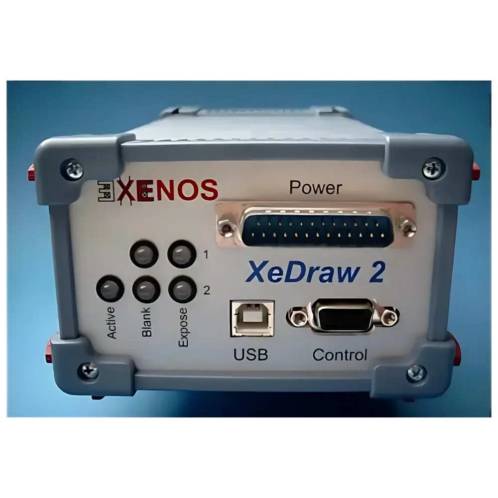
The Auniontech XENOS High-Speed Electron Beam Lithography Subsystem is a precision-engineered digital deflection control platform designed to retrofit existing scanning electron microscopes (SEM), focused ion beam (FIB), or dual-beam systems for nanoscale direct-write lithography. Unlike conventional raster-scan pattern generators, the XENOS subsystem implements real-time, hardware-accelerated beam positioning using third-order polynomial scan logic—enabling non-raster, trajectory-optimized writing of circular, elliptical, and toroidal structures without beam blanking. Its core architecture eliminates analog bandwidth-limiting components (e.g., multiplication-based DACs) in favor of fully digital field correction, ensuring distortion-free deflection signals even at maximum pixel rates of 40 MHz. The system operates on deterministic timing principles, integrating dynamic settling time computation and optimized data streaming to align with the physical bandwidth constraints of commercial SEM/FIB column electronics—making it suitable for semiconductor maskless prototyping, nanofabrication R&D, and high-resolution resist exposure in academic and industrial cleanroom environments.
Key Features
- FPGA-based real-time deflection signal generation with 16-bit or 32-bit resolution per axis
- Hardware-accelerated third-order polynomial scan engine enabling concentric ring writing and smooth parametric curve rendering
- Bandwidth-symmetric X/Y deflection logic minimizing differential lag and improving positional fidelity
- Digital field correction implemented entirely in programmable logic—no analog multipliers or calibration-dependent DACs
- Configurable logic cores and DSP firmware updatable in under five minutes via standard Ethernet interface
- Native support for industry-standard layout formats including GDSII and OASIS through integrated CAD preprocessing module
- Low-latency data pipeline with adaptive buffering to sustain 40 MHz pixel throughput without frame loss
Sample Compatibility & Compliance
The XENOS subsystem interfaces with standard SEM/FIB platforms via industry-consistent analog or digital deflection input ports (e.g., ±10 V differential, LVDS, or TTL-compatible sync lines). It supports both positive- and negative-tone electron-sensitive resists (e.g., PMMA, ZEP520A, HSQ) and is compatible with common vacuum interlocks and stage synchronization protocols. While not a standalone metrology instrument, its beam placement accuracy is traceable to SEM stage encoders and calibrated deflection amplifiers per ISO 18436-3 (Condition monitoring and diagnostics of machines) and ASTM E1558 (Standard Guide for Electron Beam Lithography). For regulated environments, the control software ECP supports audit trail logging and user access controls aligned with GLP-compliant documentation workflows.
Software & Data Management
The ECP (Electron Beam Control Platform) software suite runs natively on Linux (Ubuntu LTS) and Windows 10/11, providing GUI-driven layout import, proximity effect correction preview, dose modulation mapping, and real-time beam status monitoring. Layout preprocessing is performed offline using open-format parsers; no proprietary file lock-in is enforced. All configuration parameters—including polynomial coefficients, dwell time matrices, and settling delay tables—are stored in human-readable JSON files with SHA-256 checksums for version control. Data export supports HDF5 and CSV formats for post-processing in MATLAB, Python (NumPy/Pandas), or commercial simulation tools. Remote operation via SSH or REST API enables integration into automated fabrication workflows compliant with SEMI E142 (Equipment Communication Standard).
Applications
- Maskless lithography for MEMS/NEMS device prototyping and low-volume IC test structures
- Nanopatterning of plasmonic metasurfaces, photonic crystals, and quantum dot arrays
- Site-specific TEM lamella preparation and circuit edit in failure analysis labs
- In situ nanofabrication during SEM-based mechanical testing or environmental cell experiments
- Calibration standard generation for critical dimension SEM (CD-SEM) and scatterometry validation
- Research-grade writing of topological insulator nanostructures and 2D material heterostructure templates
FAQ
Is the XENOS subsystem compatible with my existing JEOL or Thermo Fisher SEM?
Yes—the subsystem connects via standard analog deflection inputs and supports configurable voltage scaling and offset tuning to match OEM column specifications. Integration kits include pinout documentation and signal integrity verification procedures.
Does the system require external cooling or additional power supplies?
No—it draws less than 25 W from a single 24 V DC input and operates passively cooled within standard lab ambient conditions (15–28 °C, <60% RH).
Can I import custom vector graphics or MATLAB-generated trajectories?
Yes—ECP accepts SVG path definitions and supports programmatic trajectory injection via Python bindings (included SDK) using NumPy arrays for arbitrary beam path definition.
What level of maintenance or recalibration is required?
Zero scheduled recalibration—the all-digital deflection architecture has no drift-prone analog components. Firmware updates are distributed quarterly and include backward-compatible configuration migration tools.


