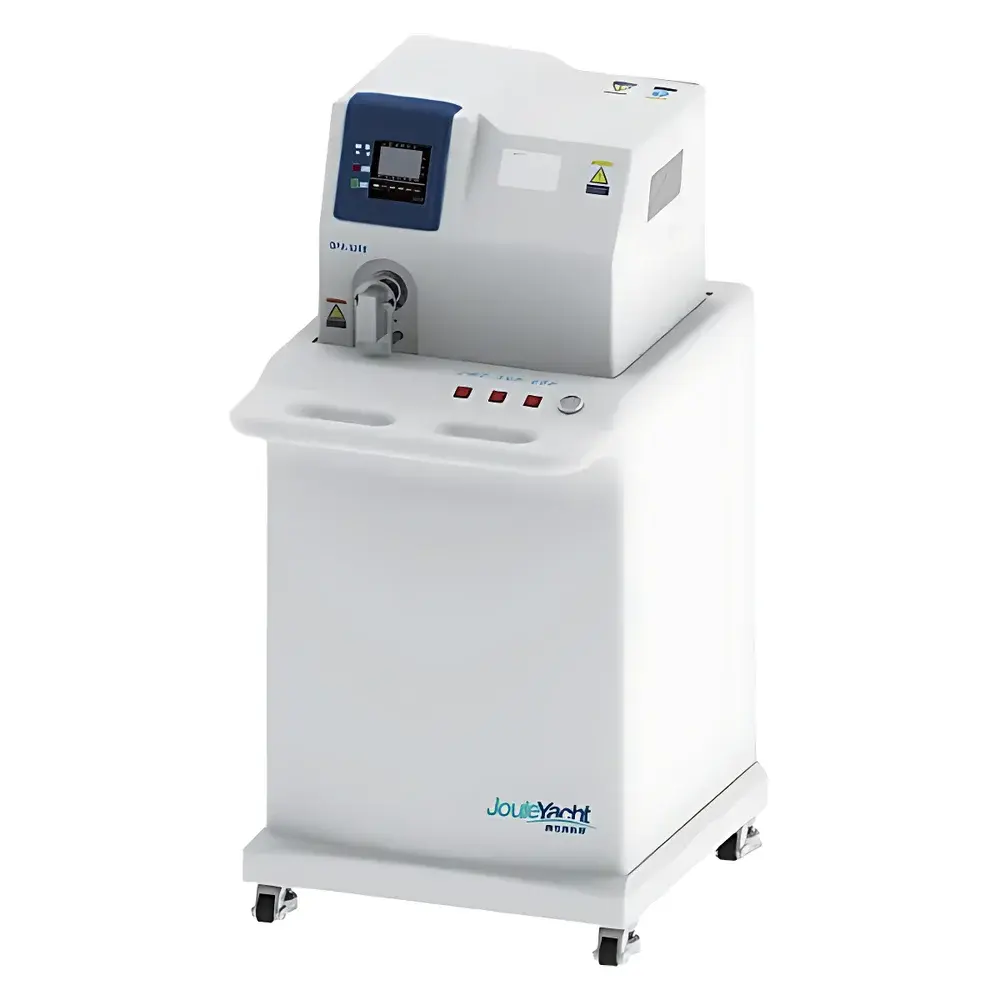
AYAO OPA Nanoscale Thin-Film Thermal Analyzer
| Brand | AYAO Instruments |
|---|---|
| Origin | Hubei, China |
| Model | OPA |
| Type | Optical Power-Based Thermal Dilatometer & Phase Transition Analyzer |
| Measurement Principle | Optical Interferometry (for thermal expansion) + Reflectance Power Monitoring (for phase transition) |
| Sample Form | Free-standing films, substrate-supported thin films, bulk materials |
| Minimum Film Thickness | 1 nm |
| Non-Destructive Testing | Yes |
| Dual-Parameter Output | Coefficient of Thermal Expansion (CTE) and Phase Transition Temperature (e.g., crystallization, melting, glass transition) |
| Compliance Context | Designed for R&D environments requiring traceable, repeatable thermal property data in accordance with ISO 11359 (thermomechanical analysis), ASTM E831 (linear thermal expansion), and GLP-aligned data integrity practices |
Overview
The AYAO OPA Nanoscale Thin-Film Thermal Analyzer is a purpose-engineered optical platform for simultaneous, non-destructive characterization of two fundamental thermophysical properties—coefficient of thermal expansion (CTE) and phase transition temperature—in ultra-thin film systems down to 1 nm thickness. Unlike conventional dilatometers or differential scanning calorimeters (DSC), the OPA leverages dual optical detection modalities: (1) high-sensitivity laser interferometry to resolve sub-nanometer dimensional changes during controlled thermal ramping, enabling precise CTE calculation for transparent or semi-transparent films on rigid substrates; and (2) real-time monitoring of reflected optical power at a fixed wavelength to detect abrupt changes in refractive index and surface morphology associated with solid–solid or solid–liquid transitions—including crystallization onset, amorphous-to-crystalline transformation, glass transition (Tg), and melting events. This hybrid architecture eliminates the need for physical contact probes or embedded sensors, preserving sample integrity and enabling repeated measurements on the same specimen across multiple thermal cycles.
Key Features
- Sub-nanometer displacement resolution via stabilized He–Ne laser interferometry, calibrated against NIST-traceable length standards
- Real-time reflectance power monitoring at 633 nm with <10 µW sensitivity, synchronized with temperature ramping (rate programmable from 0.1 to 20 K/min)
- Integrated high-stability furnace with ±0.1 K temperature uniformity over 10 mm × 10 mm sample zone
- Automated dual-parameter acquisition: CTE (α, in ppm/K) and phase transition onset/peak temperatures (°C) reported in a single run
- Vacuum-compatible chamber option (10−3 mbar base pressure) for oxidation-sensitive or low-vapor-pressure materials
- Modular sample stage supporting standard TEM grids, silicon wafers (up to 4″), and custom holders for freestanding membranes
Sample Compatibility & Compliance
The OPA accommodates a broad spectrum of thin-film architectures: sputtered or evaporated metal films (e.g., Ni, Ti, Cu), dielectric stacks (SiO2/SiNx), chalcogenide phase-change layers (Ge2Sb2Te5), polymer ultrathin films (PMMA, PS), and 2D materials (graphene, MoS2) transferred onto quartz or sapphire substrates. For opaque films, CTE determination relies on substrate curvature analysis using Stoney’s equation, while phase transitions are inferred from reflectance hysteresis loops. All measurement protocols support audit-ready documentation aligned with GLP principles; raw interferogram and photodiode voltage time-series data are timestamped and stored with full metadata (ramp rate, ambient pressure, laser power, detector gain). The system meets mechanical and electrical safety requirements per IEC 61010-1 and supports optional 21 CFR Part 11-compliant user access control and electronic signature modules.
Software & Data Management
AYAO ThermalSuite v3.2 provides instrument control, real-time visualization, and post-processing workflows. Key capabilities include baseline correction for thermal drift, derivative-based peak identification for transition temperatures, linear regression of expansion vs. temperature for CTE calculation, and overlay comparison of multiple runs. Data export formats include CSV (tabular), HDF5 (structured binary), and PDF reports with embedded uncertainty estimates (±0.5 K for Tc, ±0.2 ppm/K for α in optimized conditions). Raw datasets are automatically archived with SHA-256 checksums to ensure data provenance. Batch processing scripts (Python API included) enable high-throughput screening of combinatorial libraries or process parameter matrices.
Applications
- Optimization of annealing protocols for phase-change memory (PCM) thin films, correlating crystallization kinetics with device switching endurance
- Thermal stability assessment of perovskite photovoltaic absorbers under inert atmosphere, quantifying decomposition onset and lattice expansion prior to degradation
- CTE matching studies for heterogeneous integration of GaN-on-Si power devices, minimizing interfacial stress-induced cracking
- In situ monitoring of sol-gel derived silica films during densification, resolving shrinkage inflection points linked to network condensation
- Thermo-mechanical reliability testing of flexible OLED encapsulation barriers under thermal cycling (−40°C to +85°C, 1000 cycles)
- Validation of molecular dynamics simulations predicting thermal expansion anisotropy in van der Waals heterostructures
FAQ
Can the OPA measure thermal expansion of opaque, non-reflective films?
Yes—via substrate curvature analysis using interferometric fringe shift quantification, provided the film-substrate adhesion remains intact throughout the thermal cycle.
Is calibration required before each measurement?
No. The system performs automated self-calibration of laser wavelength and detector linearity at startup; NIST-traceable reference samples (fused silica, Invar) are recommended annually.
Does the OPA support dynamic heating profiles (e.g., step-isothermal, modulated ramps)?
Yes—ThermalSuite enables user-defined multi-segment temperature programs with dwell times, rate changes, and conditional triggers based on real-time reflectance thresholds.
What is the minimum measurable CTE value?
The detection limit is ~0.05 ppm/K for 100-nm films on 500-µm-thick fused silica substrates under optimal signal-to-noise conditions.
Are third-party software integrations supported?
Yes—native LabVIEW drivers and Python SDK (with NumPy/Pandas compatibility) are provided for integration into automated metrology workflows or MES platforms.


