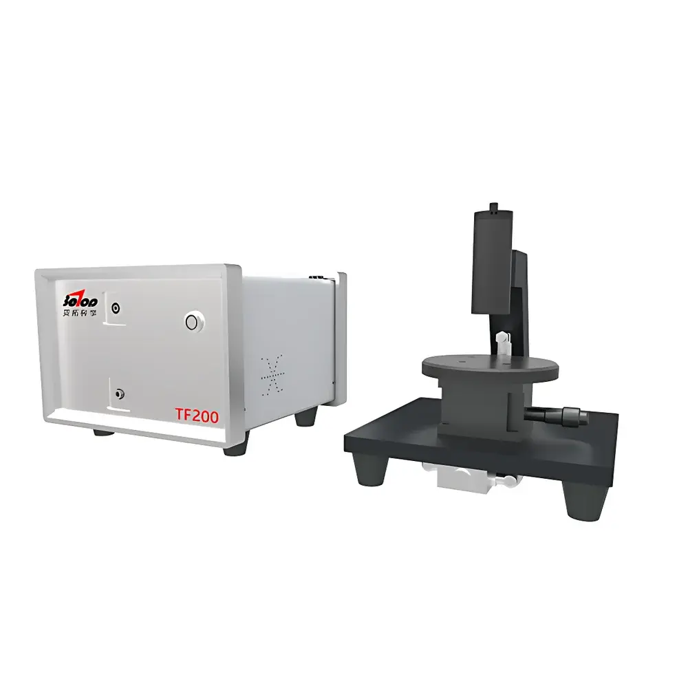
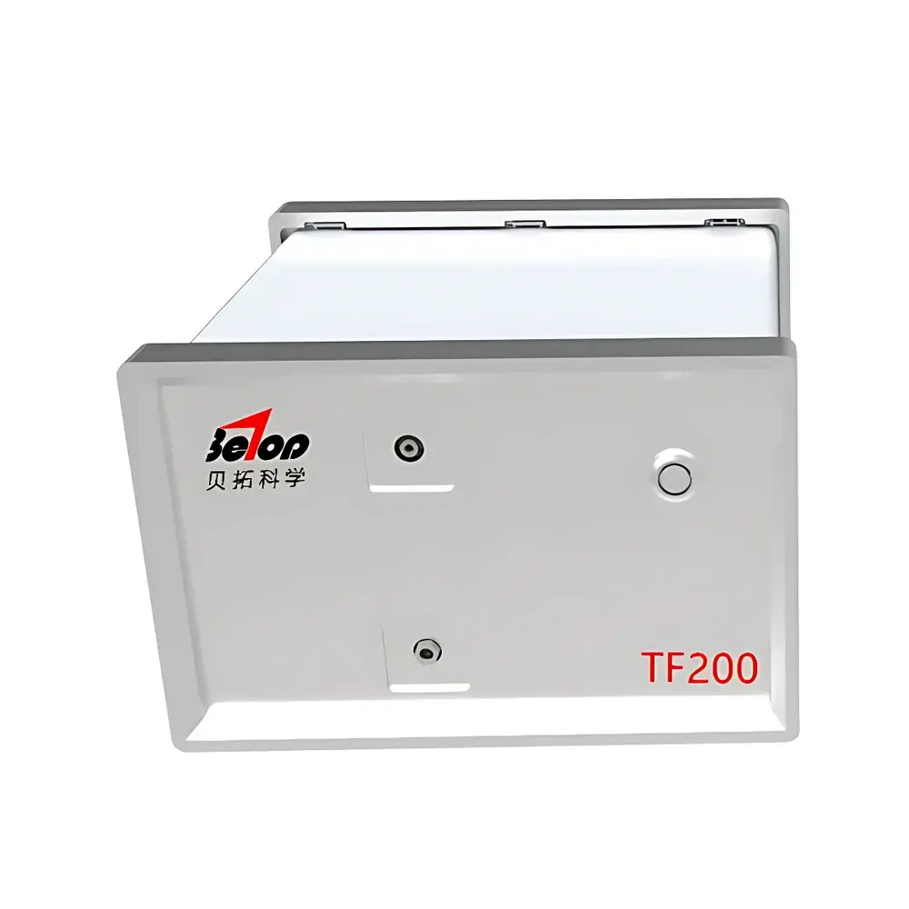
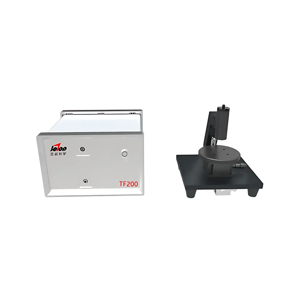
Betop Scientific TF200 White Light Interferometric Thin-Film Thickness Measurement System
| Brand | Betop Scientific |
|---|---|
| Origin | Guangdong, China |
| Manufacturer Type | Direct Manufacturer |
| Country of Origin | China |
| Model | TF200 |
| Price Range | USD 14,000 – 28,000 (FOB) |
| Wavelength Range | 380–1050 nm |
| Thickness Measurement Range | 20 nm – 40 µm |
| Thickness Accuracy | < 2 nm |
Overview
The Betop Scientific TF200 is a precision white light interferometric thin-film thickness measurement system engineered for non-contact, non-destructive characterization of single- and multi-layer optical coatings. It operates on the physical principle of spectral reflectance interference: broadband light (380–1050 nm) illuminates the sample surface at normal incidence (90°), and the spectrometer-coupled probe captures the wavelength-dependent interference pattern generated by reflections from air/film and film/substrate interfaces. Using rigorously validated inverse optical modeling algorithms—pre-calibrated against NIST-traceable reference standards—the TF200 computes film thickness with sub-nanometer resolution and high reproducibility. Unlike ellipsometry or profilometry, this method requires no vacuum environment, contact force, or conductive substrate, making it ideal for inline process monitoring and R&D labs handling delicate or temperature-sensitive samples.
Key Features
- White light interferometry-based measurement with real-time spectral acquisition and model-driven thickness inversion
- Simultaneous quantification of thickness and complex refractive index (n, k) for films >100 nm
- Four optical configurations available: TF200-VIS (380–1050 nm), TF200-EXR (380–1700 nm), TF200-DUV (190–1100 nm), and TF200-XNIR (900–1700 nm), enabling application-specific spectral coverage
- Normal-incidence optical path (90°) ensures minimal alignment sensitivity and compatibility with flat, curved, or patterned substrates
- Standard 2 mm spot size; optional micro-spot attachment supports localized analysis down to 50 µm diameter
- Integrated XY motorized stage option for automated mapping and uniformity profiling across wafers or display panels
- Fully configurable measurement modes: reflection-only, transmission-only, or combined dual-path analysis
- Designed for both benchtop lab use and integration into cleanroom-compatible production lines
Sample Compatibility & Compliance
The TF200 accommodates transparent and semi-transparent thin films on rigid or flexible substrates—including silicon, fused silica, glass, sapphire, PET, and polymer foils. It is routinely deployed in environments requiring adherence to ISO/IEC 17025-compliant calibration practices and supports GLP/GMP documentation workflows. While not inherently FDA 21 CFR Part 11-compliant out-of-the-box, its software architecture permits audit trail logging, user access control, and electronic signature implementation when configured per site-specific validation protocols. All optical components meet RoHS Directive 2011/65/EU requirements, and mechanical housing conforms to IP52 dust resistance standards.
Software & Data Management
The system ships with Betop’s proprietary TF-Measure Suite—a Windows-based application supporting intuitive workflow setup, real-time spectral visualization, multi-layer stack modeling (up to 5 layers), and batch report generation in PDF, CSV, or XML formats. Raw spectral data is stored in HDF5 format for long-term archival integrity and third-party interoperability. The software includes built-in uncertainty propagation tools that calculate total measurement uncertainty based on material dispersion models and signal-to-noise ratio (SNR) thresholds. Export modules enable direct integration with MES platforms via OPC UA or RESTful API endpoints, facilitating SPC charting and statistical process control in semiconductor fab environments.
Applications
- Semiconductor fabrication: SiO₂, SiNₓ, photoresist, SOI layer stacks, MEMS structural films
- Flat-panel display manufacturing: LCD cell gap, TFT passivation layers, ITO electrode thickness, PI alignment layers
- LED packaging: dielectric encapsulation, AR/HR coating verification, phosphor layer uniformity
- Touch sensor production: ITO trace thickness, anti-reflective hard coatings, DLC barrier layers
- Automotive optics: anti-fog polymer films, scratch-resistant hard coatings, IR-reflective solar control layers
- Medical device coatings: parylene-C on catheters/balloons, drug-eluting polymer film thickness, biocompatible hydrogel layers
FAQ
What is the minimum measurable thickness for the TF200-VIS configuration?
The TF200-VIS achieves reliable thickness quantification down to 20 nm for homogeneous single-layer films on optically contrasting substrates. For ultra-thin films (<10 nm), performance depends on substrate reflectivity and spectral SNR.
Can the TF200 measure opaque or metallic films?
No—it requires at least partial optical transparency or semi-transparency in the selected wavelength band. Opaque metal layers (e.g., bulk Al or Cu) are outside its operational scope unless used as underlying reflective substrates for overlying dielectrics.
Is calibration required before each measurement?
Factory calibration is stable for ≥12 months under controlled lab conditions. Daily verification using certified reference wafers (e.g., Si/SiO₂ standards) is recommended for GMP-aligned operations.
Does the system support automated wafer-level scanning?
Yes—when equipped with the optional XY translation stage and alignment fiducial recognition module, the TF200 can execute full-wafer thickness maps with ≤5 µm positional repeatability.
How is measurement uncertainty reported?
Uncertainty is calculated per ASTM E2821–19 guidelines and includes contributions from spectral noise, dispersion model error, and interface roughness estimation—typically expressed as ±(0.4% of reading or 2 nm), whichever is greater.