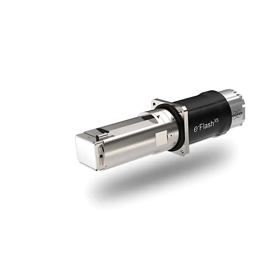
Bruker e-Flash XS EBSD System for Compact SEM
| Brand | Bruker |
|---|---|
| Origin | Germany |
| Manufacturer Type | Authorized Distributor |
| Import Status | Imported |
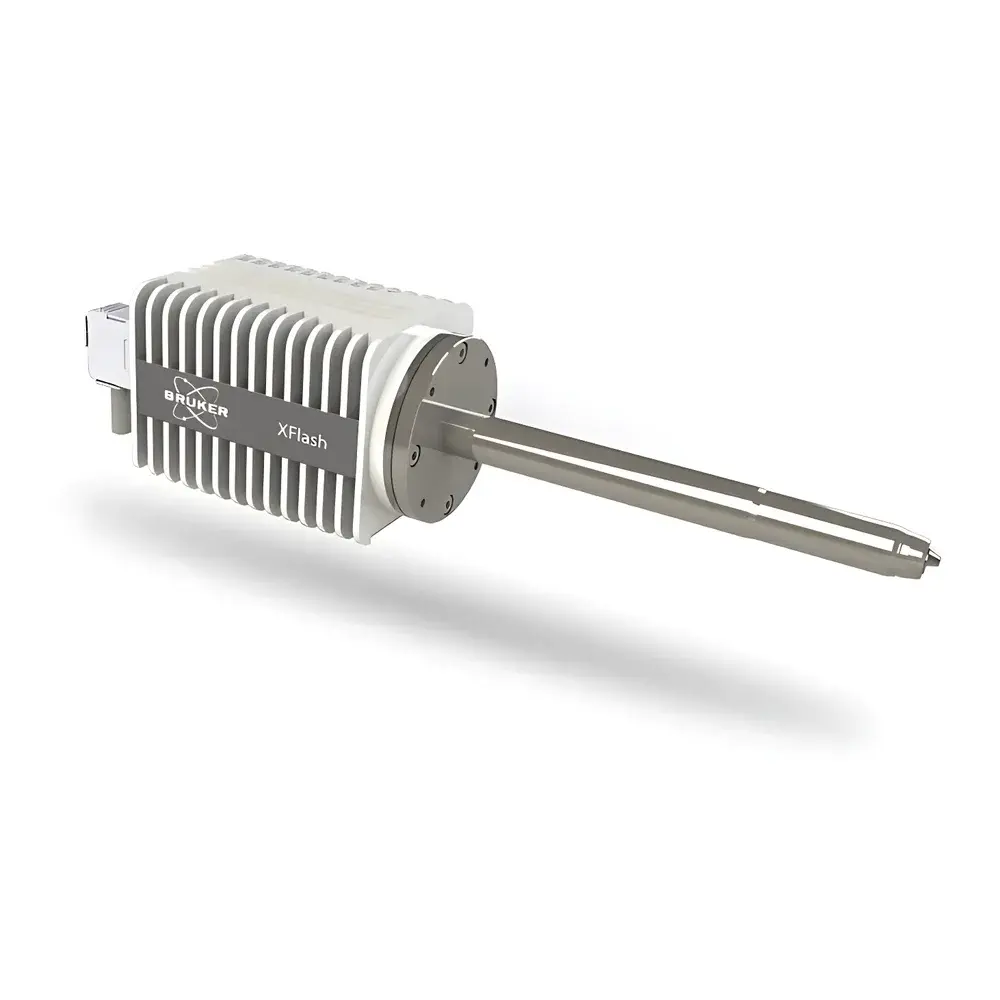
| Model | QUANTAX ED-XS |
| CCD Camera Resolution | 640 × 480 pixels |
| Maximum Stage Speed | 10 mm/s |
| Spatial Resolution | 50 nm |
| Angular Resolution | 0.2° |
Overview
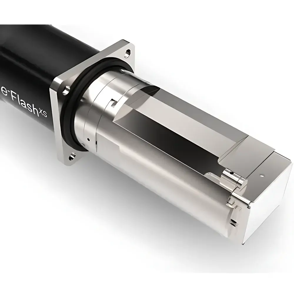
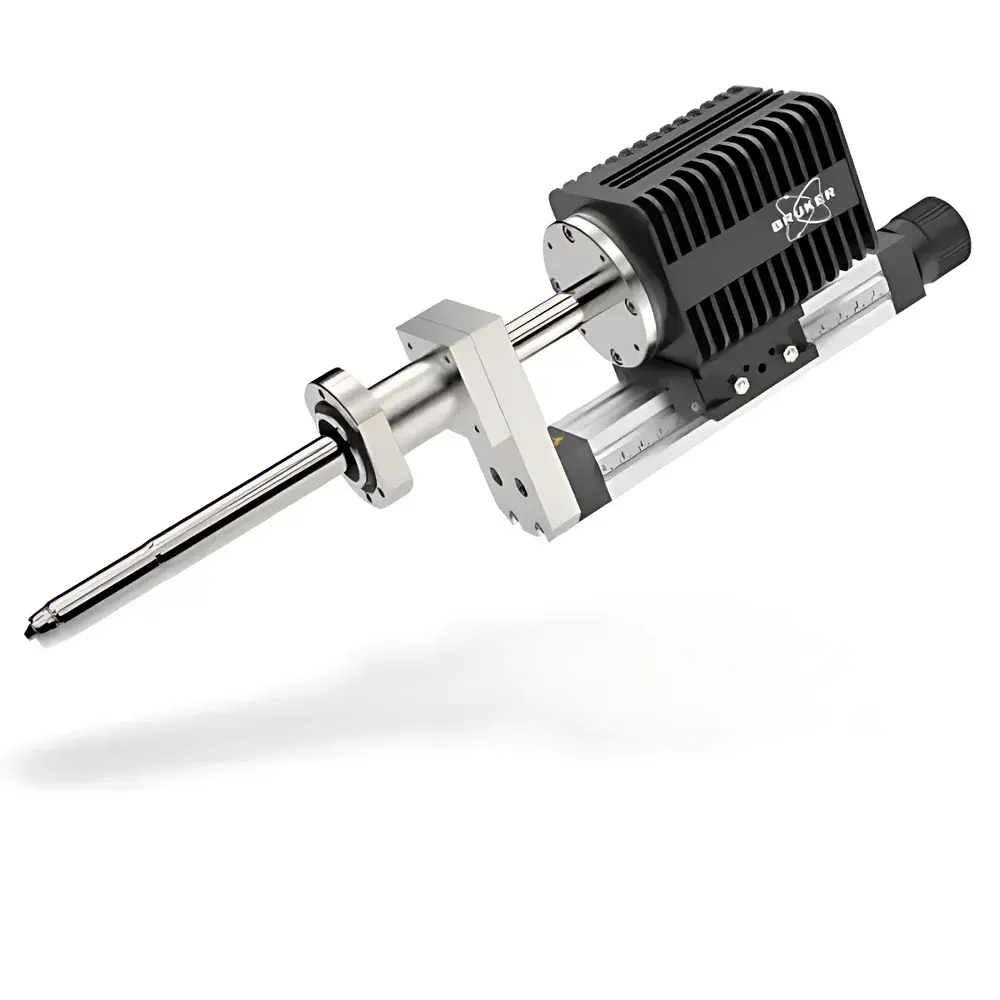
The Bruker e-Flash XS EBSD system is a purpose-engineered electron backscatter diffraction (EBSD) solution designed specifically for integration with compact scanning electron microscopes (SEM), including benchtop and low-voltage SEM platforms. Operating on the fundamental principle of elastic scattering of high-energy electrons at crystalline lattice planes, the system captures Kikuchi diffraction patterns from the sample surface under tilted beam conditions. These patterns are indexed in real time to generate crystallographic orientation maps, phase identification, grain boundary characterization, and strain distribution data. Unlike conventional EBSD detectors requiring complex alignment or vacuum-compatible phosphor screens, the e-Flash XS utilizes a robust, retractable detector architecture that maintains full compatibility with standard SEM chamber configurations—enabling rapid installation, minimal downtime, and zero interference with other in-chamber accessories such as EDS detectors or STEM holders.
Key Features
- Compact, modular design optimized for space-constrained SEM chambers—including benchtop and entry-level field-emission SEMs.
- Fully retractable detector mechanism ensures mechanical safety: when retracted, the e-Flash XS occupies no active chamber volume, eliminating collision risk with EDS detectors, stage components, or manipulators (0% probability of accidental contact during routine operation).
- No user calibration required: factory-aligned optical path and pre-characterized phosphor screen enable immediate pattern acquisition upon installation.
- Integrated phosphor screen replacement capability—users can swap screens without breaking vacuum or involving service engineers—reducing operational overhead and extending system uptime.
- Synchronized EBSD–EDS data acquisition via Bruker’s unified QUANTAX platform, supporting concurrent collection of crystallographic and elemental information from identical scan positions.
- High angular resolution of 0.2° enables reliable detection of sub-micron grain rotations, deformation twins, and low-angle boundaries in metals, ceramics, and geological specimens.
Sample Compatibility & Compliance
The e-Flash XS supports standard EBSD sample geometries: flat, polished, conductive specimens tilted at 70° ± 2° relative to the incident beam. It is compatible with common polishing protocols (e.g., colloidal silica final polish for metals) and charge-compensation techniques for non-conductive materials. The system complies with ISO/IEC 17025 requirements for measurement traceability in accredited laboratories and supports audit-ready metadata logging per GLP and GMP frameworks. All acquired diffraction patterns, indexing confidence indices, and orientation solutions are timestamped and stored with instrument configuration parameters—ensuring full data provenance for regulatory submissions (e.g., ASTM E112, ISO 13067, USP ).
Software & Data Management
Controlled through Bruker’s ESPRIT software suite, the e-Flash XS provides intuitive workflow navigation—from automated pattern acquisition and Hough-based indexing to advanced post-processing (grain reconstruction, misorientation analysis, kernel average misorientation mapping). Raw pattern files (.tif/.hdf5) and processed results (.csv, .ctf, .ang) are natively exportable for third-party analysis (MTEX, Channel 5, OIM Analysis). The software includes built-in 21 CFR Part 11 compliance modules: electronic signatures, role-based access control, and immutable audit trails for all processing steps and parameter modifications—essential for pharmaceutical, aerospace, and nuclear QA/QC environments.
Applications
- Microstructural characterization of additive-manufactured alloys: grain morphology, texture evolution, and epitaxial growth tracking across build layers.
- Failure analysis of turbine blades and weld joints: identification of strain localization zones, slip system activity, and recrystallization behavior under thermal-mechanical loading.
- Geological sample analysis: quantification of crystal preferred orientation (CPO) in olivine and quartz aggregates for tectonic strain modeling.
- Thin-film semiconductor metrology: determination of epitaxial quality, mosaic spread, and interfacial misfit dislocation density in III–V heterostructures.
- Quality assurance in battery electrode manufacturing: correlation of particle orientation with Li-ion diffusion anisotropy in NMC and LFP cathodes.
FAQ
Is vacuum interruption required to replace the phosphor screen?
No. The phosphor screen is user-replaceable without venting the SEM chamber or removing the detector from the port.
Can EBSD and EDS data be collected simultaneously on the same scan grid?
Yes. The QUANTAX ED-XS platform synchronizes beam scanning, pattern acquisition, and X-ray detection at the pixel level—ensuring spatially registered crystallographic and compositional datasets.
What is the minimum detectable grain size with this system?
Grains as small as ~100 nm can be resolved under optimal preparation and beam conditions, leveraging the 50 nm spatial resolution and 0.2° angular precision.
Does the system support automated phase identification in multi-phase samples?
Yes. ESPRIT includes a library-based pattern matching engine trained on >1,200 ICDD PDF-4+ crystal structures, enabling unambiguous phase discrimination in complex composites and intermetallics.
Is remote diagnostics and software update support available?
Yes. Bruker’s SecureLink remote access protocol allows authorized engineers to perform firmware updates, diagnostic checks, and configuration optimization while maintaining full data security and network isolation compliance.


