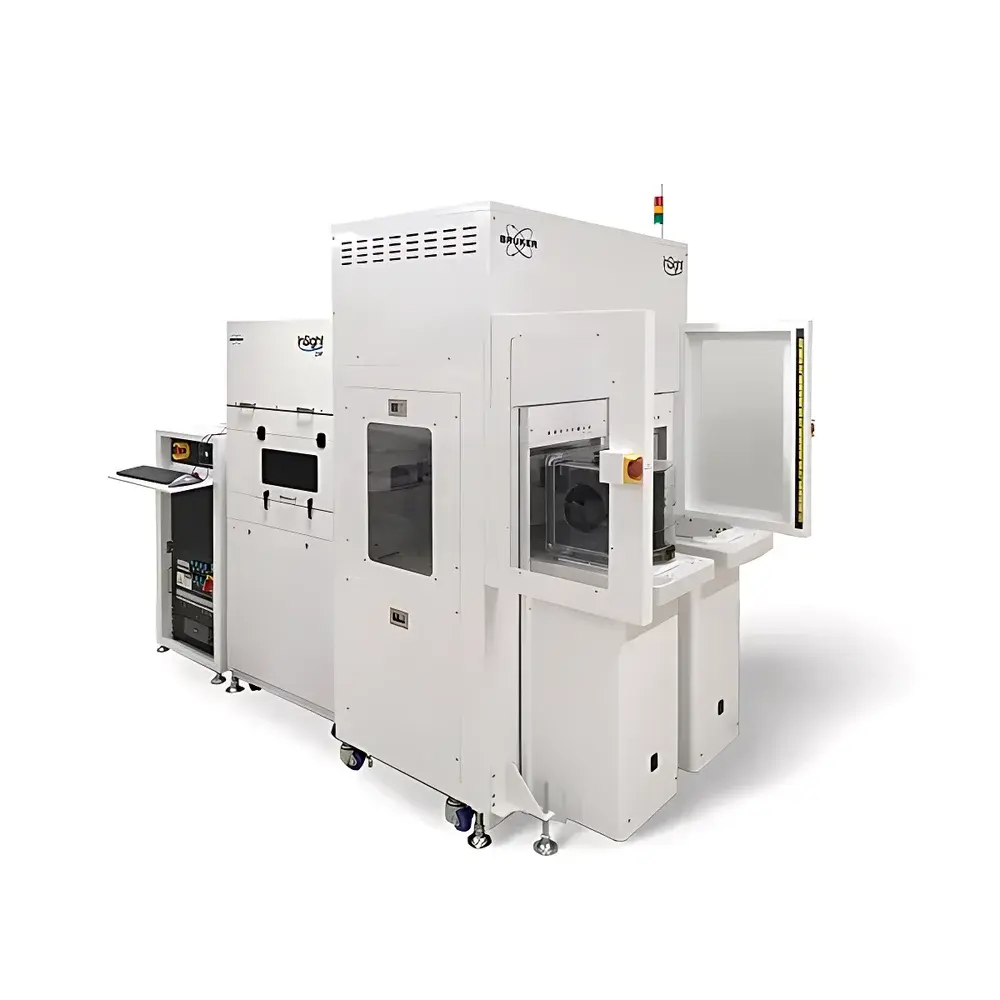
Bruker InSight CAP Automated Atomic Force Microscope
| Brand | Bruker |
|---|---|
| Origin | USA |
| Manufacturer Type | Authorized Distributor |
| Origin Category | Imported |
| Model | InSight CAP |
| Price Range | USD $180,000 – $240,000 |
| Instrument Type | Atomic Force Microscope (AFM) |
| Application Class | Industrial Metrology System |
| XY Positioning Noise | < 65 nm (RMS, 0.1–10 Hz) |
| Maximum Sample Size | 33 mm × 26 mm |
| Stage Travel Range | 100 mm × 300 mm (X × Y) |
| Scan Range | 65 µm × 65 µm (XY), up to 15 µm (Z) |
| Long-Term Dynamic Repeatability | < 0.5 nm |
| Surface Flatness Accuracy over 26 mm | < 20 nm PV |
| AFM Controller | NanoScope® V 64-bit Digital Signal Processor |
Overview
The Bruker InSight CAP is an industrial-grade, fully automated atomic force microscope engineered for high-precision, in-line metrology in semiconductor manufacturing environments. Unlike conventional AFMs designed for academic or general R&D use, the InSight CAP integrates a purpose-built scanning architecture with advanced motion control and real-time adaptive feedback to deliver sub-nanometer surface topography characterization under production-relevant conditions. Its core measurement principle relies on dynamic-mode (tapping-mode) AFM with laser-interferometric Z-sensor feedback, enabling quantitative height mapping with Ångström-level vertical resolution and exceptional long-term stability. The system is specifically optimized for post-CMP (Chemical Mechanical Planarization) and etch process monitoring—critical for advanced logic and memory nodes where nanoscale planarity, local dishing, erosion, and step-height uniformity directly impact lithographic focus depth and device yield.
Key Features
- Automated wafer handling and alignment compatible with 100 mm to 300 mm substrates via configurable stage integration (manual load, semi-automated cassette interface, or full factory automation-ready).
- NanoScope® V 64-bit controller architecture delivering 5× faster probe engagement and 5× improved approach speed versus prior-generation systems—reducing cycle time without compromising data fidelity.
- DT (Dynamic Tracking) adaptive scan mode that dynamically adjusts scan parameters in real time to maintain optimal tip–sample interaction during high-speed profiling of topographically complex surfaces.
- Enhanced mechanical stability with <65 nm RMS XY positioning noise (0.1–10 Hz bandwidth), ensuring reproducible traceability across repeated measurements and multi-shift operations.
- Sub-0.5 nm long-term dynamic repeatability verified per ASTM E2527 and ISO/IEC 17025-compliant calibration protocols—enabling direct use in SPC (Statistical Process Control) workflows.
- Integrated flatness metrology package supporting PV, RMS, and SFQ (Spatial Frequency Quantification) analysis over fields up to 26 mm, aligned with SEMI D39 and JEDEC JESD22-A108 standards for CMP validation.
Sample Compatibility & Compliance
The InSight CAP accommodates rigid, flat substrates up to 33 mm × 26 mm in footprint—ideal for reticle inspection, mask blank metrology, and diced die evaluation. While optimized for silicon wafers, it supports quartz, sapphire, SiC, and low-k dielectric films with appropriate cantilever selection (e.g., conductive Pt/Ir or ultra-low-noise silicon nitride probes). All hardware and firmware comply with CE marking requirements (EMC Directive 2014/30/EU, Low Voltage Directive 2014/35/EU) and meet IEC 61326-1:2013 for industrial electromagnetic immunity. Data acquisition and reporting are structured to support GLP/GMP audit trails and FDA 21 CFR Part 11 compliance when deployed with Bruker’s optional secure software suite and electronic signature modules.
Software & Data Management
Operation is managed through Bruker’s NanoScope Analysis v2.0 platform, a Windows-based application featuring scriptable batch processing, cross-platform data exchange (Gwyddion-compatible .wsx, ISO-standard .xyz, and HDF5 export), and integrated statistical reporting. The software includes dedicated modules for CMP-specific metrics—including dishing ratio, erosion depth, within-die non-uniformity (WDNU), and edge exclusion zone (EEZ) analysis—as defined in SEMI P35 and ITRS roadmap guidelines. Raw AFM data streams are timestamped, checksum-verified, and stored with full metadata (probe ID, calibration date, environmental logs) to satisfy traceability requirements in ISO 9001:2015-certified fabs.
Applications
- Post-CMP surface flatness verification for EUV lithography readiness (targeting <20 nm PV over 26 mm fields).
- Quantitative characterization of shallow trench isolation (STI) topography and gate oxide step heights.
- Etch profile metrology including sidewall angle, line edge roughness (LER), and bottom CD uniformity on patterned wafers.
- Thin-film thickness and interfacial roughness assessment for ALD/CVD layers in advanced packaging and 3D NAND stacks.
- Failure analysis of micro-defects such as residual slurry particles, pad-induced scratches, and localized delamination.
FAQ
Is the InSight CAP compatible with 300 mm wafer handling systems?
Yes—when integrated with optional robotic interface modules (SEMI E47.1 compliant), the InSight CAP supports front-end-of-line (FEOL) and back-end-of-line (BEOL) metrology stations in automated 300 mm fabrication lines.
What probe types are recommended for high-resolution CMP metrology?
Bruker recommends RTESP-300 (Si, k = 40 N/m) for general-purpose dishing/erosion mapping and HA_NC (conductive diamond-coated, k = 2.8 N/m) for low-force, high-resolution dielectric film profiling.
Does the system support automated tip qualification and calibration?
Yes—the NanoScope V controller performs in situ thermal tune and sensitivity calibration before each scan sequence, and optional tip wear monitoring is available via real-time amplitude-phase tracking.
Can measurement data be exported to factory MES or SPARK systems?
Yes—via OPC UA server integration or CSV/JSON API endpoints, enabling seamless transfer of metrology results into Fab-wide data lakes and statistical control platforms.
What is the typical measurement throughput for a full 26 mm × 26 mm flatness map?
At standard 1024 × 1024 pixel resolution and 2 Hz line rate, a full-field map requires ~8–12 minutes; DT mode reduces this by up to 40% while preserving <0.1 nm RMS noise floor.


