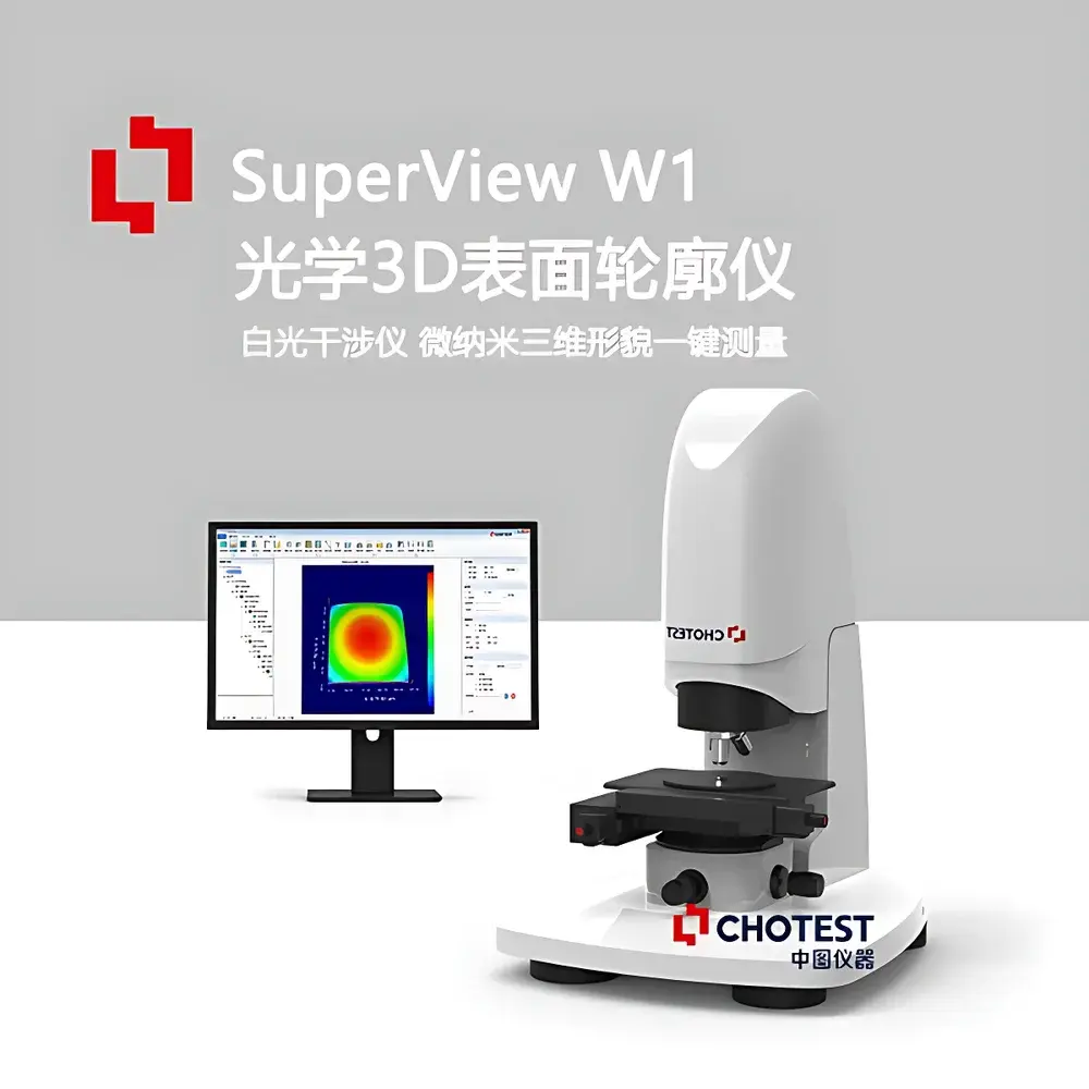
Chotest SuperView W402 Nanoscale 3D White-Light Interferometric Profilometer
| Brand | Chotest |
|---|---|
| Model | W402 |
| Light Source | White LED |
| Imaging Sensor | 1024 × 1024 pixels |
| Standard Objective | 10× (optional: 2.5×, 5×, 20×, 50×, 100×) |
| Zoom Lens | 0.5× standard (optional: 0.375×, 0.75×, 1×) |
| FOV (10×) | 0.98 × 0.98 mm |
| XY Stage | 140 × 100 mm travel, 320 × 200 mm footprint, 10 kg load capacity |
| Z Focus Range | 100 mm motorized |
| Vertical Resolution | ≤ 0.1 nm (environmental noise evaluation mode) |
| Surface Reflectivity Range | 0.05% – 100% |
| Dimensions (H×W×D) | 900 × 700 × 600 mm |
| Vibration Isolation | Active air-bearing optical table base |
Overview
The Chotest SuperView W402 is a high-precision, non-contact 3D white-light interferometric profilometer engineered for nanoscale topographic characterization of functional surfaces across research, quality control, and advanced manufacturing environments. It operates on the principle of white-light scanning interferometry (WLSI), where broadband illumination generates localized interference fringes at the point of zero optical path difference (OPD) between reference and measurement beams. By precisely tracking fringe contrast maxima across vertical scan positions, the system reconstructs surface height with sub-nanometer vertical resolution and lateral resolution governed by the diffraction limit of the selected objective lens. Unlike conventional phase-shifting interferometry (PSI), which suffers from limited unambiguous measurement range (~λ/4), or vertical scanning interferometry (VSI), which trades off axial resolution for dynamic range, the W402 implements an adaptive EPSI (Enhanced Phase-Shifting Interferometry) reconstruction algorithm—enabling simultaneous high-resolution profiling over extended vertical ranges (up to 100 mm Z-travel) without phase ambiguity or stitching artifacts. This makes it uniquely suited for measuring complex micro-structured surfaces including ultra-smooth concave aspheres, MEMS mirrors, semiconductor wafers, optical coatings, and biomedical implants.
Key Features
- Universal sample compatibility: Single-scan mode supports quantitative profiling of surfaces ranging from super-polished (Rq < 0.1 nm) to highly scattering or absorptive (e.g., black silicon, transparent thin films, matte ceramics) without manual exposure or gain adjustment.
- Automated multi-point metrology: One-click execution of stripe search, vertical scan, and focus optimization across user-defined single or arrayed measurement sites—including rectangular, circular, ring-shaped, or spiral grid patterns.
- Seamless large-area stitching: Supports automated mosaic acquisition and alignment of >1,000 individual fields-of-view using real-time image navigation and sub-pixel registration algorithms; eliminates overlap gaps and edge discontinuities in reconstructed topographies.
- Programmable workflow engine: Enables full integration of measurement, filtering, feature extraction, and analysis steps into reusable scripts—ideal for routine inspection of standardized components under ISO/IEC 17025 or IATF 16949-compliant QA processes.
- Comprehensive environmental monitoring: Integrated 0.1 nm-resolution vibration diagnostics module quantifies amplitude and frequency spectra of ambient mechanical noise, supporting root-cause analysis during GLP/GMP validation or facility qualification.
- Dual-layer hardware protection: Combines software-enforced Z-stop limits with mechanical pressure-sensing and spring-loaded objective lens carriage to prevent collision-induced damage during manual or automated operation.
- Intelligent illumination management: Automatic LED dimming and shutdown after configurable idle time preserves source lifetime and thermal stability—critical for long-duration drift-critical measurements.
Sample Compatibility & Compliance
The W402 accommodates samples up to 10 kg on its motorized XY stage, with programmable positioning repeatability better than ±0.5 µm. Its wide reflectivity tolerance (0.05–100%) enables direct measurement of challenging materials such as silicon nitride MEMS membranes, indium tin oxide (ITO) electrodes, polymer-based microfluidic channels, and oxidized metal alloys—without conductive coating or vacuum requirements. The instrument complies with electromagnetic compatibility (EMC) standards IEC 61326-1 and safety standard IEC 61010-1. All data acquisition, processing, and reporting functions are designed to support audit trails compliant with FDA 21 CFR Part 11 when deployed in regulated pharmaceutical or medical device manufacturing settings. Traceable calibration certificates per ISO/IEC 17025 are available upon request.
Software & Data Management
The proprietary MetroPro X platform provides a unified interface for acquisition, visualization, and analysis. It supports hierarchical project organization, version-controlled parameter templates, and batch processing of datasets against predefined analysis protocols. Raw interferograms and reconstructed height maps are stored in vendor-neutral HDF5 format with embedded metadata (timestamp, objective ID, environmental conditions, operator ID). Export options include PDF reports with annotated cross-sections and statistical summaries, Excel-compatible CSV files containing Ra, Rq, Rz, Sa, Sq, curvature, volume, and feature-count metrics, and high-fidelity TIFF exports for third-party finite element modeling (FEM) or CAD reverse engineering workflows. Audit trail logs record all user actions—including parameter changes, filter applications, and report generation—with timestamps and digital signatures.
Applications
The W402 serves critical metrology needs in optics fabrication (surface figure error of lenses and mirrors), semiconductor process control (CMP uniformity, trench depth, via profile), precision machining (tool wear assessment, surface integrity after EDM or laser ablation), additive manufacturing (powder bed roughness, layer fusion defects), and biomaterials (implant surface texture, scaffold porosity, cell-adhesion topography). It meets ASTM E2942 (standard guide for 3D surface topography measurement), ISO 25178-2 (areal surface texture parameters), and USP <1059> (optical surface characterization for parenteral containers). Typical use cases include quantifying polishing-induced subsurface damage on fused silica optics, validating replication fidelity in nanoimprint lithography molds, and assessing corrosion-induced pitting morphology on stainless steel surgical instruments.
FAQ
What is the minimum resolvable surface height difference?
The system achieves ≤ 0.1 nm vertical resolution under controlled environmental conditions (Class 1000 cleanroom, active vibration isolation), verified via NIST-traceable step-height standards.
Can the W402 measure transparent thin films on substrates?
Yes—its broadband coherence gating allows separation of interference signals from air/film and film/substrate interfaces, enabling thickness and interfacial roughness measurement of films down to ~50 nm.
Is offline analysis possible without the instrument connected?
Yes—MetroPro X supports full post-processing of saved datasets on standalone workstations, including custom script execution and report generation.
How is calibration maintained across different objectives and magnifications?
Each objective is factory-characterized for pixel scale, telecentricity error, and chromatic aberration; calibration coefficients are auto-loaded based on objective identification via integrated RFID tags.
Does the system support G-code or external motion controller integration?
Yes—via TCP/IP API and optional EtherCAT interface, enabling synchronization with CNC stages, robotic arms, or inline production line triggers for automated in-process inspection.


