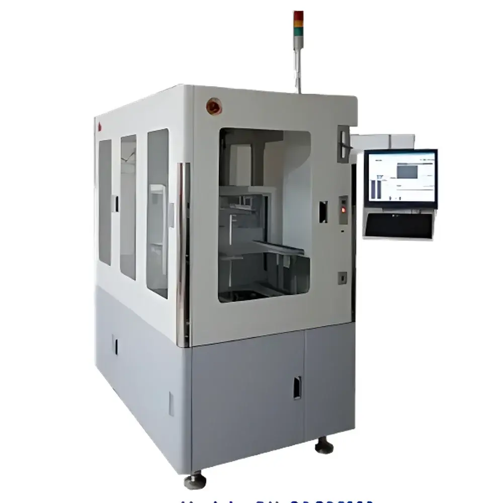
DAIN HITECH DH-OBCP5000 Automatic Wafer OCR Labeling System
| Brand | DAIN HITECH |
|---|---|
| Origin | South Korea |
| Model | DH-OBCP5000 |
| Wafer Compatibility | 6", 8", 12" (flat & notch) |
| OCR Recognition Rate | ≥99.8% |
| Throughput | 90 wafers/hour (12" standard orientation) |
| Printing Method | Thermal Transfer |
| Print Resolution | 305 dpi |
| Max Print Speed | 150 mm/s |
| Label Dimensions | 22–131 mm (W) × 6–356 mm (L) |
| ESD Protection | <100 V (10 s) |
| Acoustic Noise | ≤70 dB(A) |
| UPS Backup Duration | 3 min |
| Safety | Dual emergency stop buttons, magnetic safety sensors on all access doors |
| Software Features | MES integration (T-card scanning), dual-label printing mode, post-print barcode verification, server-based auto-backup, wafer mapping synchronization |
Overview
The DAIN HITECH DH-OBCP5000 Automatic Wafer OCR Labeling System is an industrial-grade semiconductor front-end automation solution engineered for high-accuracy, non-contact identification and traceability labeling of silicon wafers during pre-dicing preparation. It integrates optical character recognition (OCR), machine vision, thermal-transfer barcode printing, and precision mechanical handling to establish unambiguous wafer-level data linkage between physical substrates and factory execution systems (MES). Unlike manual or semi-automated labeling approaches, the DH-OBCP5000 performs full-cycle label generation—including ID extraction from native wafer surface markings (e.g., laser-etched alphanumeric codes), geometric alignment, position-adaptive label placement, and post-application verification—without mechanical contact or surface stress. Its architecture conforms to cleanroom-compatible design principles (ISO Class 5 compliant airflow management optional), with ESD-safe materials and grounding paths meeting JEDEC JESD625-B requirements for static-sensitive semiconductor handling.
Key Features
- High-fidelity OCR engine optimized for low-contrast, rotated, or partially obscured wafer IDs—supports flat (6″, 8″) and notch-type (8″, 12″) substrates with automatic orientation compensation.
- Thermal-transfer barcode printer with 305 dpi resolution and programmable label positioning (0°, 90°, 180°, 270°) relative to wafer ring geometry, ensuring consistent registration across cassette-based workflows.
- Dual-mode labeling operation: Mode 1 executes label print-and-apply upon successful OCR read; Mode 2 initiates label generation after T-card scan and MES data pull, enabling synchronized lot-level metadata embedding (e.g., process history, layer stack, test results).
- Integrated vision-based verification module confirms barcode legibility and positional accuracy immediately after application—rejecting misaligned or unreadable labels in real time.
- Full ESD control: Conductive chassis, grounded chuck, ionized air assist (optional), and <100 V discharge retention per ANSI/ESD S20.20—validated for Class 0 device handling.
- Modular transport interface supports both manual cassette loading and automated integration via SMIF or FOUP load ports (retrofit kit available).
- Comprehensive audit trail: All OCR events, print commands, verification outcomes, and user actions are timestamped and logged with operator ID—supporting GLP/GMP-aligned record retention and FDA 21 CFR Part 11 electronic signature readiness when deployed with validated software configuration.
Sample Compatibility & Compliance
The DH-OBCP5000 accommodates industry-standard wafer formats including 150 mm (6″), 200 mm (8″), and 300 mm (12″) substrates—both flat-edge and notch-edge configurations. It handles bare silicon, oxide-coated, nitride-passivated, and photoresist-patterned wafers without risk of micro-scratching or particle generation, verified per SEMI F47-0218 mechanical stress testing. The system complies with CE machinery directive 2006/42/EC, electromagnetic compatibility per EN 61326-1, and occupational noise limits per ISO 4871. Optional ISO 14644-1 Class 5 laminar flow enclosures are available for integration into controlled environments.
Software & Data Management
Controlled via a Windows-based HMI with intuitive touchscreen interface, the DH-OBCP5000 firmware includes native support for SECS/GEM communication protocols (SECS-II HSMS over TCP/IP), enabling direct handshake with MES, AMHS, and host equipment controllers. All labeling operations generate structured XML logs containing wafer ID, timestamp, camera exposure parameters, OCR confidence score, print coordinates, and verification pass/fail status. Logs are automatically archived to network file shares or SQL databases with configurable retention policies. Optional validation packages include IQ/OQ documentation, cybersecurity hardening (NIST SP 800-53 controls), and 21 CFR Part 11 compliance add-ons covering electronic signatures, audit trail immutability, and role-based access control (RBAC).
Applications
- Pre-dicing traceability setup for backend assembly lines (e.g., die attach, wire bonding)
- Wafer sort and probe station integration—mapping correlation between electrical test data and physical location
- Lot genealogy tracking in compound semiconductor fabs (GaAs, SiC, GaN)
- Quality gate enforcement prior to packaging—ensuring only wafers with verified ID and complete metrology history proceed downstream
- Automated rework loop management: relabeling wafers returning from defect review or repair stations
FAQ
Does the DH-OBCP5000 support multi-language OCR for wafers marked in Korean, Chinese, or Japanese characters?
Yes—the OCR engine includes UTF-8 character set expansion and can be trained on customer-specific font libraries, including non-Latin glyphs commonly used in Asian fab ID conventions.
Can the system interface with legacy MES platforms lacking SECS/GEM?
Yes—via configurable CSV/FTP polling or OPC UA gateway modules, enabling bidirectional data exchange with older manufacturing systems.
Is the thermal-transfer printer compatible with chemical-resistant label stock required for wet bench environments?
Yes—standard configuration accepts polyester (PET) and polyimide (PI) label media rated for HF, HNO₃, and acetone exposure per MIL-STD-130N Annex C.
What maintenance intervals are recommended for the vision system and print head?
Camera lens calibration: quarterly; print head cleaning: daily (automated wipe cycle); ribbon and label roll replacement: per consumables usage log—average service life exceeds 20,000 labels per thermal printhead.
How is alignment accuracy verified during qualification?
Using NIST-traceable reticle targets and coordinate measuring machine (CMM) cross-checks—typical positional repeatability is ±0.15 mm at 95% confidence across full 12″ wafer ring travel range.


