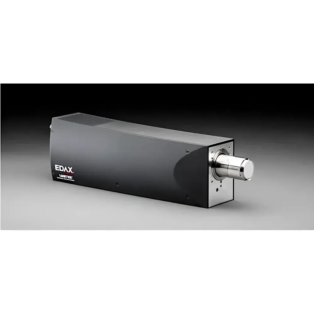
EDAX Hikari XP Electron Backscatter Diffraction (EBSD) Detector System
| Brand | EDAX |
|---|---|
| Origin | USA |
| Model | Hikari XP |
| Angular Resolution | < 0.1° |
| Maximum Pattern Indexing Rate | up to 1400 points/sec |
| Beam Current Compatibility | down to 100 pA |
| Accelerating Voltage Compatibility | down to 5 kV |
Overview
The EDAX Hikari XP Electron Backscatter Diffraction (EBSD) Detector System is a high-performance, field-emission scanning electron microscope (FE-SEM)–integrated crystallographic characterization platform engineered for precision orientation mapping, phase identification, and microstructural analysis at sub-micron to nanoscale resolutions. Unlike conventional EBSD detectors constrained by the historical trade-off between acquisition speed and pattern sensitivity, the Hikari XP employs a proprietary low-noise, high-dynamic-range CMOS sensor architecture coupled with optimized phosphor-scintillator optics and real-time pattern processing firmware. This enables simultaneous high-speed indexing—up to 1400 indexed points per second—and exceptional sensitivity under low-dose conditions (beam currents as low as 100 pA and accelerating voltages down to 5 kV), making it suitable for beam-sensitive materials, thin films, and nanostructured specimens. Its core measurement principle relies on the detection and indexing of Kikuchi diffraction patterns generated by backscattered electrons interacting with crystalline lattices, providing quantitative orientation data with angular resolution better than 0.1°, essential for strain mapping, grain boundary characterization, and texture analysis in metallurgy, geoscience, semiconductor, and advanced ceramics research.
Key Features
- Unified performance architecture eliminating the traditional compromise between speed and sensitivity—enables both high-throughput mapping and nanoscale indexing without hardware reconfiguration
- Three-tiered model scalability: Hikari Pro (600 pts/sec), Hikari Plus (1000 pts/sec), and Hikari Super (1400 pts/sec), all sharing identical optical and electronic design for consistent data quality across throughput tiers
- Integrated Front-Side Detector (FSD) for rapid pre-scan assessment of sample topography, phase distribution, and orientation contrast prior to EBSD acquisition—reducing setup time and improving ROI selection accuracy
- Patented Confidence Index (CI) algorithm embedded in TEAM™ software, delivering not only indexing success rate but also per-pixel reliability metrics—critical for GLP-compliant reporting and traceable microstructural interpretation
- Native compatibility with PRIAS™ (Pattern Region Imaging and Analysis System), enabling synchronized acquisition of up to 25 region-of-interest (ROI)-specific images—including orientation, phase, and topographic contrast—in real time during EBSD mapping
- Robust signal-to-noise optimization across full SEM operating ranges, validated for stable performance from ultra-low beam currents (100 pA) to standard analytical conditions (≥1 nA)
Sample Compatibility & Compliance
The Hikari XP system supports a broad spectrum of conductive and non-conductive crystalline materials—including metals, alloys, intermetallics, oxides, silicates, and polycrystalline semiconductors—when prepared using standard EBSD-compatible techniques (e.g., ion milling, electropolishing, or low-angle Ar⁺ sputtering). Its low-voltage and low-beam-current capability extends applicability to radiation-sensitive phases (e.g., battery cathode materials, organic-inorganic hybrids) and electron-transparent TEM lamellae analyzed in dual-beam FIB-SEM systems. The detector complies with ISO/IEC 17025 requirements for calibration traceability of angular resolution and indexing fidelity. Data acquisition workflows are fully auditable under FDA 21 CFR Part 11 when deployed with TEAM™ software configured for electronic signatures, audit trails, and user-access controls—supporting GMP/GLP-regulated R&D environments in aerospace, medical device, and pharmaceutical materials development.
Software & Data Management
Hikari XP operates exclusively within EDAX’s TEAM™ software ecosystem—including TEAM™ Trident (for correlative EDS/EBSD), TEAM™ Pegasus (for high-resolution phase mapping), and TEAM™ EBSD (for standalone orientation analysis). All versions support automated drift correction, dynamic background subtraction, grain reconstruction with misorientation thresholding, and lattice strain quantification via high-order harmonic fitting. Raw pattern files are stored in vendor-neutral HDF5 format with embedded metadata (beam energy, working distance, stage coordinates, CI values), ensuring long-term archival integrity and third-party interoperability (e.g., MTEX, EMsoft, or Python-based pyEBSDindex pipelines). Batch processing, scripting via Python API, and export to ASTM E112-compliant grain size reports enable seamless integration into enterprise LIMS and QMS platforms.
Applications
- Quantitative texture analysis in rolled aluminum alloys and Ni-based superalloys for hot-working process optimization
- In-situ deformation studies tracking dislocation cell formation, twin nucleation, and subgrain rotation under mechanical loading in SEM stages
- Phase transformation kinetics mapping in heat-treated steels, including martensite-austenite partitioning and retained austenite quantification
- Grain boundary engineering in additively manufactured Ti-6Al-4V to correlate build parameters with Σ3 twin density and crack propagation resistance
- Microstructural homogeneity assessment of geological thin sections for tectonic strain history reconstruction
- Failure analysis of solder joints and interconnects in microelectronics packaging, combining EBSD orientation data with EDS elemental maps
FAQ
What distinguishes Hikari XP from previous-generation EBSD detectors?
Hikari XP replaces the legacy speed-versus-sensitivity dichotomy with a single architecture that delivers both high indexing rates (up to 1400 pts/sec) and high pattern fidelity at low beam doses—eliminating the need for separate “high-speed” or “high-sensitivity” detector configurations.
Is Hikari XP compatible with non-EDAX SEM platforms?
Yes—Hikari XP interfaces with major SEM manufacturers (Thermo Fisher Scientific, Zeiss, JEOL, Hitachi) via standard PCIe-based detector control modules and calibrated stage synchronization protocols; full functionality requires TEAM™ software installation.
How does the Confidence Index improve data reliability?
The CI metric is derived from pattern matching residuals and neighbor consistency checks—not merely signal intensity—providing statistically grounded confidence thresholds for each indexed pixel, enabling objective filtering and uncertainty-aware microstructural modeling.
Can Hikari XP perform automated phase identification without prior reference patterns?
While reference pattern libraries (e.g., ICDD PDF-4+) are required for unambiguous phase assignment, TEAM™ software includes unsupervised clustering tools (e.g., PCA + k-means) that group similar patterns for exploratory phase discovery prior to library matching.
What maintenance or recalibration is required for long-term angular resolution stability?
The system features factory-calibrated geometric distortion correction and thermal drift compensation; annual verification against NIST-traceable Si or Ni reference standards is recommended for ISO 17025 compliance, with no user-serviceable optical alignment needed.


