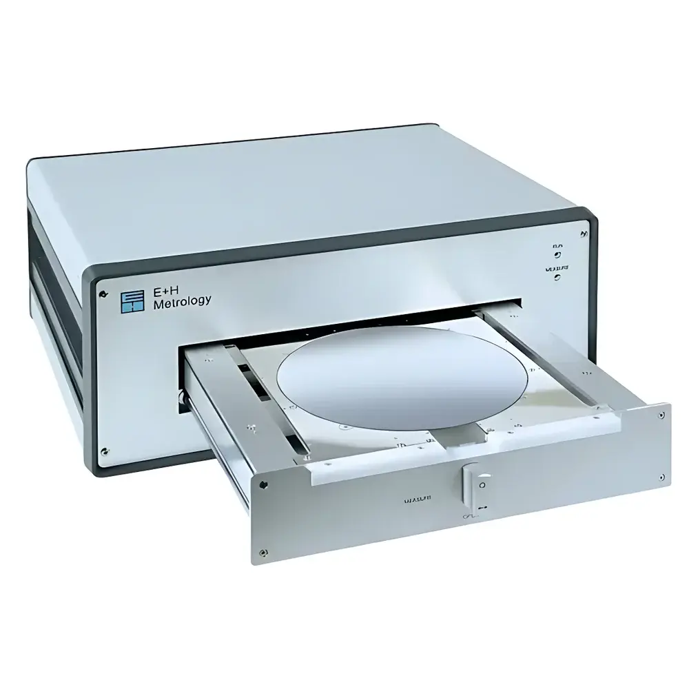
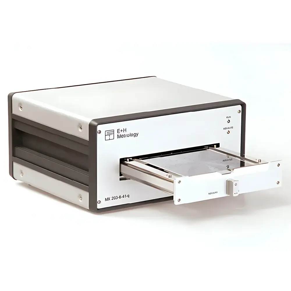
Endress+Hauser MX 203 Manual Wafer Thickness & Topography Metrology System
| Brand | Endress+Hauser Metrology |
|---|---|
| Country of Origin | Germany |
| Manufacturer Type | Authorized Distributor |
| Product Origin | Imported |
| Model | MX 203 |
| Pricing | Upon Request |
| Wafer Diameter Range | 50 mm – 450 mm (2″ – 18″) |
| Thickness Accuracy | ±0.5 µm |
| Thickness Resolution | 50 nm |
| Thickness Measurement Range | 100 µm – 1000 µm |
| Measurement Principle | Dual-Sided Capacitive Sensing |
| Automation Level | Manual Operation |
| Compatible Substrates | Si, SiC, GaN, GaAs, InP |
Overview
The Endress+Hauser MX 203 is a high-precision manual metrology system engineered for non-contact, dual-sided capacitive measurement of semiconductor wafers. Designed specifically for front-end process control and quality assurance in R&D, pilot-line, and low-volume production environments, the MX 203 delivers traceable, repeatable characterization of critical geometric parameters—including thickness, Total Thickness Variation (TTV), Bow, Warp, and stress-induced surface topography. Its operational principle relies on parallel-plate capacitive sensing: two opposing sensor arrays—mounted above and below the wafer—measure minute changes in capacitance as a function of distance between each sensor and the wafer surface. By simultaneously acquiring spatially resolved distance data across both surfaces, the system reconstructs absolute thickness at discrete points and computes derived metrics per SEMI MF-1530, SEMI MF-1391, and ISO 14407 standards. The MX 203 supports full-diameter scanning with user-defined grid density (up to 100×100 points), enabling quantitative mapping of surface deviation and curvature without mechanical contact or vacuum chucking—critical for fragile, ultra-thin, or warped substrates.
Key Features
- Dual-axis capacitive sensor architecture with temperature-stabilized electronics for long-term drift compensation
- Calibration traceable to national metrology institutes (e.g., PTB, NIST) via certified reference wafers and step-height standards
- Manual Z-stage with micrometer-driven vertical positioning and integrated tactile homing switch for reproducible sensor-to-wafer standoff
- Modular sensor head design accommodating wafer diameters from 50 mm (2″) to 450 mm (18″) using interchangeable mounting fixtures
- Real-time thickness deviation visualization with color-mapped contour plots and cross-sectional line profiles
- Integrated environmental monitoring: onboard temperature and humidity sensors log ambient conditions during acquisition for thermal drift correction
- Rugged aluminum-alloy frame with vibration-damped optical table interface, compliant with ISO 20486 cleanroom compatibility requirements
Sample Compatibility & Compliance
The MX 203 is validated for use with bare and processed wafers composed of silicon (Si), silicon carbide (SiC), gallium nitride (GaN), gallium arsenide (GaAs), and indium phosphide (InP). It accommodates both polished and epitaxial layers, oxidized or nitrided surfaces, and thin-film-coated substrates—provided dielectric properties remain within defined permittivity bounds (εr = 3–12). The system conforms to SEMI standards MF-1530 (Wafer Thickness Measurement), MF-1391 (Total Thickness Variation), and MF-1832 (Stress Calculation from Bow/Warp). All measurement procedures support GLP-compliant documentation: audit trails record operator ID, calibration status, environmental logs, and raw sensor data timestamps. While not FDA 21 CFR Part 11–certified out-of-the-box, the software architecture permits integration with validated LIMS or MES platforms supporting electronic signatures and change control.
Software & Data Management
The MX 203 operates under Endress+Hauser’s proprietary WaferScan Pro v4.x software suite, delivered on a Windows 10 IoT Enterprise platform. The application provides guided workflows for setup, calibration, scan definition, and report generation. Raw capacitance values are stored in HDF5 format with embedded metadata (sensor gain, offset, temperature, timestamp, coordinate mapping). Export options include CSV (for statistical process control), STEP AP242 (for CAD-integrated tolerance analysis), and PDF/HTML reports compliant with internal QA templates. Data integrity safeguards include write-once storage mode, automatic checksum validation, and optional network-based backup to secure NAS infrastructure. Software updates follow IEC 62443-2-4 security guidelines, with signed firmware packages and role-based access control (RBAC) for configuration-level permissions.
Applications
- Pre- and post-CMP thickness uniformity verification for Si and compound semiconductor wafers
- Process development feedback for epitaxial growth, ion implantation, and annealing cycles
- Qualification of reclaimed wafers and edge-trimmed substrates prior to reuse
- Stress profiling of heteroepitaxial layers (e.g., GaN-on-Si) to identify delamination risk zones
- Reference metrology for validating automated inline thickness tools (e.g., ellipsometers, interferometers)
- Failure analysis labs requiring sub-micron TTV resolution without vacuum or backside coating requirements
FAQ
Does the MX 203 require vacuum or backside contact to measure warped wafers?
No. The dual-capacitive architecture measures absolute distance from each sensor to its respective wafer surface independently; no mechanical contact, vacuum chucking, or backside preparation is needed.
Can the system measure wafers with conductive films or metal layers?
Yes—provided the film thickness is ≤100 nm and resistivity exceeds 10⁴ Ω·cm. Thicker or highly conductive layers may attenuate the electric field; empirical validation with representative samples is recommended.
Is calibration performed in-house or only by Endress+Hauser service centers?
Field calibration using certified reference wafers is supported. Full sensor alignment and drift characterization require factory service, available globally through authorized metrology partners.
What is the typical measurement time for a full 300 mm wafer at 50×50 point density?
Approximately 180 seconds, including stage settling, sensor stabilization, and data acquisition—excluding manual loading/unloading.
Does the software support custom formula definitions for derived parameters (e.g., stress calculation with substrate-specific Young’s modulus)?
Yes. WaferScan Pro includes a scripting module (Python 3.9 embedded) allowing users to define and deploy custom algorithms within the reporting pipeline.


