Eoptics SE-VF Spectroscopic Ellipsometer
| Brand | Eoptics |
|---|---|
| Origin | Hubei, China |
| Manufacturer Type | Authorized Distributor |
| Country of Origin | China |
| Model | SE-VF |
| Pricing | Upon Request |
Overview
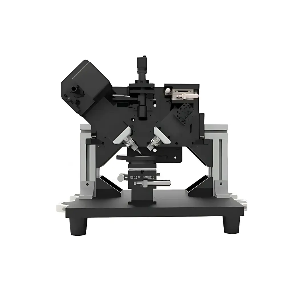
The Eoptics SE-VF Spectroscopic Ellipsometer is a high-precision, research-grade optical metrology instrument engineered for non-destructive, contactless characterization of thin-film optical constants (refractive index n, extinction coefficient k) and physical thickness (d) on patterned microstructures. Operating on the fundamental principle of spectroscopic ellipsometry—measuring the change in polarization state of reflected broadband light across a defined spectral range (typically 240–1700 nm)—the SE-VF delivers quantitative, model-based analysis of multilayer stacks on semiconductor wafers, display substrates, and photonic devices. Its design prioritizes micro-scale spatial resolution and rapid acquisition, making it especially suitable for inline process monitoring and R&D applications where feature sizes fall below 50 µm and throughput demands exceed conventional scanning ellipsometers.
Key Features
- Micro-Spot Capability: Equipped with motorized, software-controlled focusing optics enabling user-defined spot sizes down to 30 µm (FWHM), optimized for measurements on lithographically defined features such as gate trenches, metal interconnects, and pixelated OLED layers.
- High-Speed Acquisition: Achieves full-spectrum ellipsometric data collection (Ψ and Δ) in under 500 ms per measurement point, supporting real-time process feedback and high-density mapping without compromising signal-to-noise ratio.
- Modular Configuration: Offers scalable hardware options including automated XYZ θ-stage integration, environmental chamber compatibility (N₂ purge, temperature control), and optional rotating analyzer or compensator configurations for enhanced Mueller matrix capability.
- Compact Form Factor: Engineered with a low-profile optical head and minimized footprint (≤ 450 × 350 × 280 mm), facilitating seamless integration into cleanroom tool clusters, vacuum load-lock interfaces, or benchtop metrology stations.
- Stable Optical Architecture: Utilizes fused silica broadband optics, thermally stabilized halogen/deuterium light source, and high-resolution CCD spectrometer with grating selection to ensure long-term photometric stability and wavelength calibration traceability.
Sample Compatibility & Compliance
The SE-VF supports measurement on transparent and semi-transparent substrates—including fused silica, sapphire, BK7 glass, and silicon-on-insulator (SOI)—with film systems ranging from single-layer anti-reflection coatings (e.g., SiO₂, MgF₂) to complex stacks involving ITO, TiN, Al₂O₃, and organic emissive layers. It complies with ISO 15504-2 (optical thin-film measurement standards) and supports traceable calibration protocols aligned with NIST-traceable reference samples. While not certified for GMP production environments out-of-the-box, its software architecture accommodates audit-ready operation when deployed with optional 21 CFR Part 11-compliant electronic signatures and full audit trail logging.
Software & Data Management
Controlled via Eoptics’ proprietary EllipSoft™ v4.x platform, the SE-VF provides intuitive workflow management—from automated alignment routines and multi-point grid mapping to advanced regression analysis using Levenberg-Marquardt optimization. The software includes built-in optical dispersion models (Cauchy, Tauc-Lorentz, Cody-Lorentz), layer stack editors with interface roughness and grading parameters, and batch processing for statistical process control (SPC). Export formats include CSV, XML, and HDF5; raw spectra and fit residuals are stored with metadata (date/time, operator ID, instrument configuration) to support GLP documentation requirements.
Applications
- Process development and qualification of ALD, PVD, and CVD-deposited films in semiconductor front-end-of-line (FEOL) and back-end-of-line (BEOL) fabrication.
- Optical constant extraction for transparent conductive oxides (TCOs) used in touch sensors and solar cells.
- Thickness uniformity mapping across 200 mm and 300 mm wafers, including edge exclusion analysis.
- Characterization of sub-100 nm dielectric layers in MEMS and integrated photonics platforms.
- Quality assurance of optical coatings on AR/HR mirrors, laser optics, and biomedical sensor substrates.
FAQ
What spectral range does the SE-VF cover?
The standard configuration operates from 240 nm to 1700 nm, with optional extension to 210 nm (vacuum UV) or 2500 nm (NIR) upon request.
Can the SE-VF measure rough or textured surfaces?
Yes—it supports effective medium approximation (EMA) modeling for surface roughness and graded interfaces, though measurement accuracy decreases for RMS roughness exceeding 5% of film thickness.
Is remote operation supported?
EllipSoft™ includes TCP/IP API and LabVIEW driver support, enabling integration with factory automation systems (SECS/GEM) and centralized metrology data platforms.
Does the system require periodic recalibration?
Annual wavelength and intensity calibration is recommended using certified reference standards; daily verification with a Si/SiO₂ reference wafer is advised for production-critical use.
What sample stage options are available?
Standard configurations include manual XY translation; motorized stages with ±0.1 µm repeatability, auto-focus, and wafer handling (up to 300 mm) are available as OEM modules.


