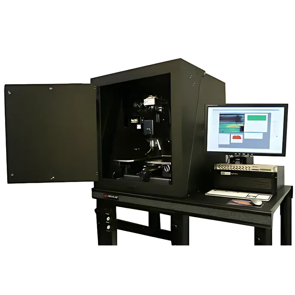
FAI Crystal Vision Emission Microscope (EMMI)
| Brand | FAI |
|---|---|
| Origin | USA |
| Manufacturer Type | Authorized Distributor |
| Import Status | Imported |
| Model | FAI Crystal Vision |
| Pricing | Upon Request |
Overview
The FAI Crystal Vision Emission Microscope (EMMI) is a high-sensitivity, cryogenically cooled optical imaging system engineered for failure analysis of semiconductor devices at the sub-micron level. It operates on the principle of photon emission detection—capturing ultra-low-intensity light (photons) and thermal radiation generated by defect-related recombination, hot-carrier injection, gate oxide breakdown, latch-up, or Joule heating in integrated circuits under electrical bias or laser stimulation. Unlike conventional optical microscopes, the Crystal Vision EMMI integrates multi-spectral detection capabilities across UV–VIS–NIR–SWIR bands, enabling correlative analysis of electroluminescence (EL), photoluminescence (PL), thermally induced emission, and stimulus-induced fault signatures—all within a single platform. Designed for use in semiconductor reliability labs, failure analysis centers, and advanced packaging R&D environments, it supports both front-side and back-side inspection of packaged and unpackaged ICs, wafers, and bare die.
Key Features
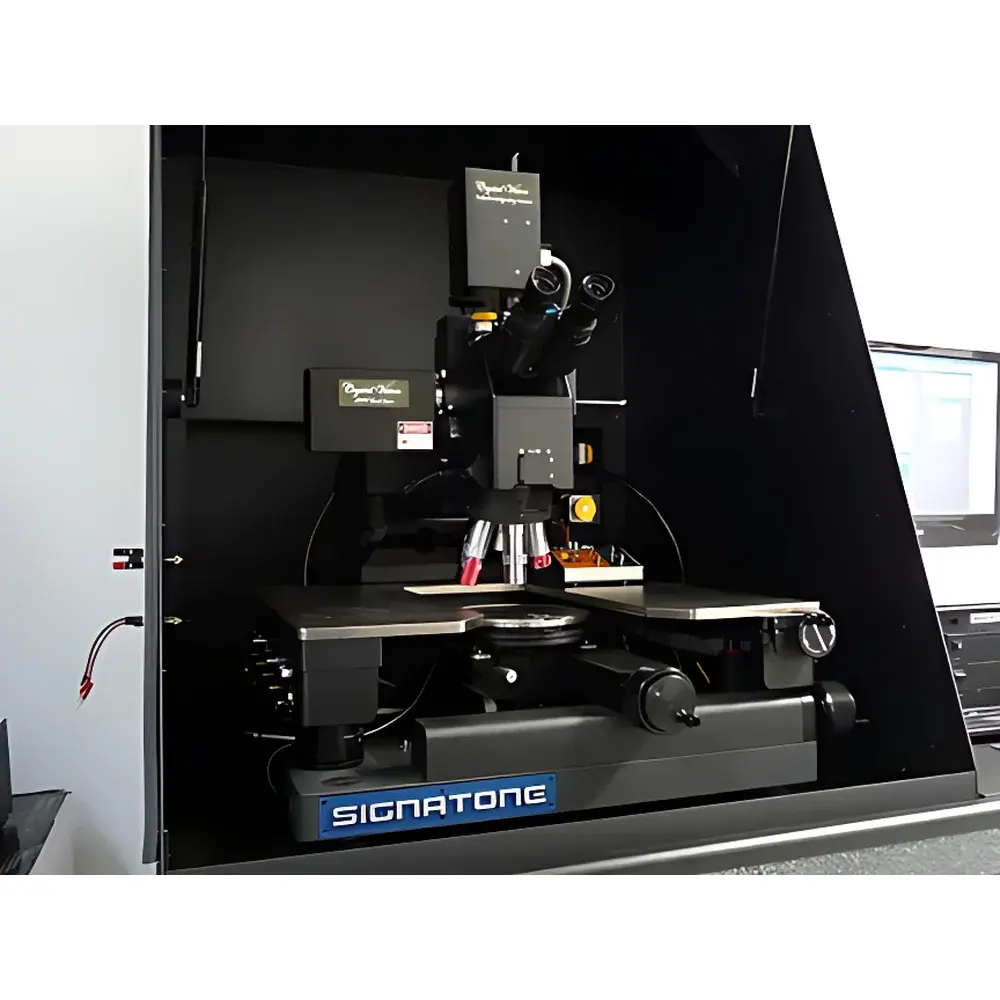
- Modular detector architecture supporting concurrent or sequential integration of up to four independent detectors: CCD, InGaAs, VisGaAs, and optional thermal imaging modules.
- TEC-cooled CCD detector with spectral response from 365 nm to 1190 nm; operating temperature stabilized below –40 °C without liquid nitrogen; 1280 × 1024 resolution; dark current <0.002 e⁻/s; read noise <7 e⁻; exposure range: 32 ms to 2 hours.
- High-sensitivity InGaAs detector covering 900–1750 nm; 320 × 240 resolution; 30 µm × 30 µm pixel pitch; quantum efficiency >80% (950–1700 nm); NEI <1 × 10¹⁰ ph/cm²/s; exposure range: 1 µs to 60 minutes.
- VisGaAs hybrid detector spanning 500–1800 nm—eliminating the need for separate CCD and InGaAs units while maintaining deep-cooling performance (≤ –40 °C).
- Dual-wavelength SIFT (Stimulus-Induced Fault Testing) laser scanning head with 654 nm and 1428 nm sources; constant-current feedback control ensures stable biasing during laser stimulation and prevents overvoltage damage.
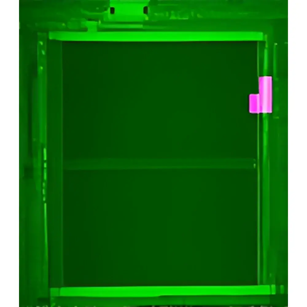
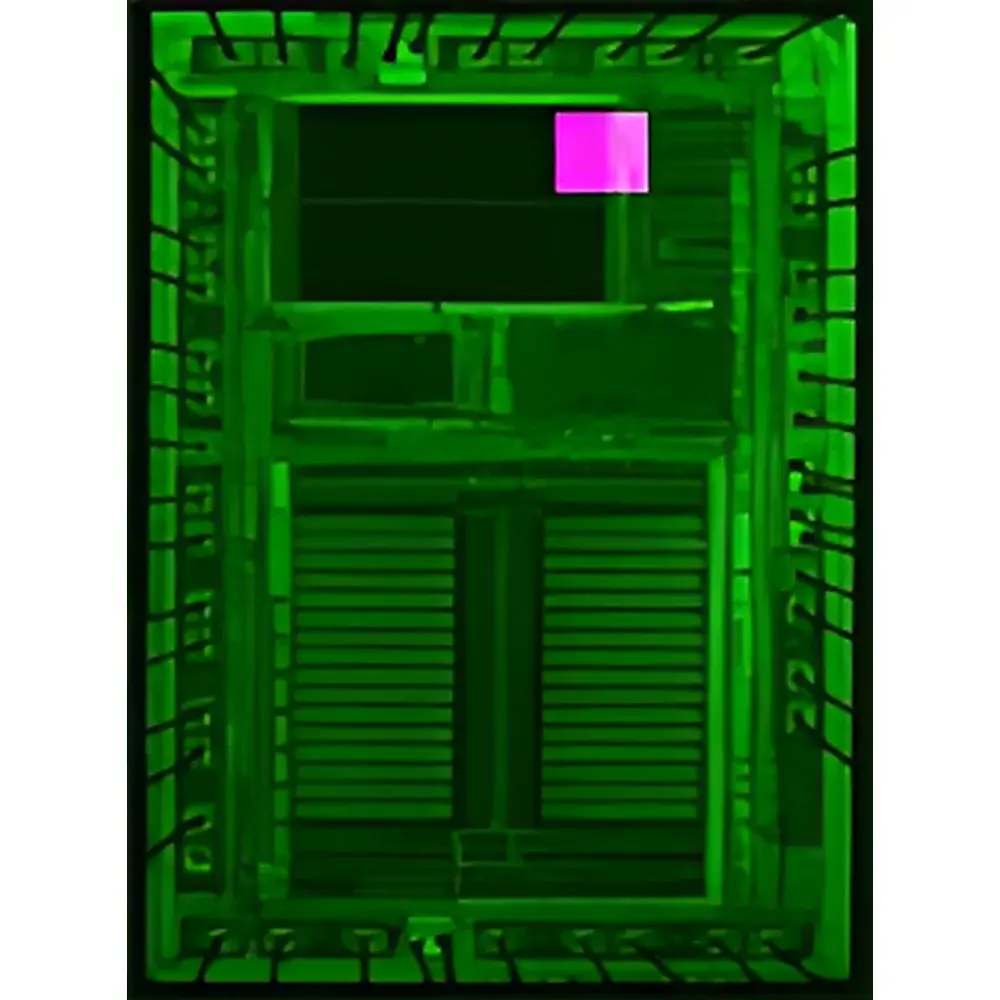
- FMI (Fluorescence-based Microthermal Imaging): non-contact thermal resolution of 1 mK at ambient temperature; no liquid crystal media required.
- SLC (Stabilized Liquid Crystal) thermal imaging module offering 10 mK thermal resolution; optimized for high-contrast, real-time thermal mapping of power dissipation anomalies.
- Moire-based backside thermal imaging: enables nanoscale thermal gradient detection through silicon substrates using interferometric fringe pattern analysis.
Sample Compatibility & Compliance
The Crystal Vision EMMI accommodates a broad range of semiconductor samples—including flip-chip BGA packages, wire-bonded QFNs, wafer-level CSPs, and thinned silicon substrates down to 50 µm thickness. Its motorized XYZ stage, precision Z-height calibration, and automated focus tracking support repeatable positioning for cross-platform correlation with SEM, FIB, or OBIRCH systems. The system complies with industry-standard failure analysis workflows defined in JEDEC JESD22-A108, JEDEC JESD22-A115, and ASTM F1718. Data acquisition and reporting modules are designed to meet GLP and GMP documentation requirements, including full audit trail logging and user-access controls aligned with FDA 21 CFR Part 11 principles.
Software & Data Management
The proprietary Crystal Vision Analysis Suite provides synchronized multi-detector image acquisition, time-resolved photon counting, spectral overlay registration, and spatially resolved intensity profiling. Real-time SIFT signal correlation overlays laser scan position with emission intensity maps, enabling direct localization of leakage paths or weak oxide regions. All raw data—including TIFF stacks, metadata headers (exposure, gain, cooling status, laser parameters), and ROI annotations—are stored in vendor-neutral HDF5 format. Export options include CSV, PNG, and MATLAB-compatible .mat files. Software supports batch processing, script-driven automation via Python API, and integration with enterprise LIMS platforms through RESTful web services.
Applications
- Identification of gate oxide shorts, junction leakage, and latch-up sites in CMOS and FinFET technologies.
- Localization of electromigration voids and resistive open faults in interconnect layers.
- Analysis of ESD-induced damage in I/O protection structures and transient voltage suppressors.
- Correlation of photonic emission with dynamic power supply noise in high-speed SerDes and RF transceivers.
- Thermal mapping of hotspot evolution during burn-in stress testing or accelerated life testing.
- Backside failure localization in 2.5D/3D stacked die configurations using Moire interferometry and SWIR transmission imaging.
FAQ
What is the minimum detectable photon flux for the InGaAs detector?
The InGaAs detector achieves a noise-equivalent irradiance (NEI) of <1 × 10¹⁰ photons/cm²/s across its operational band, enabling detection of single-event photon bursts under optimized bias and cooling conditions.
Can the system perform simultaneous dual-detector acquisition?
Yes—the Crystal Vision platform supports hardware-synchronized acquisition from two detectors (e.g., CCD + InGaAs) using shared timing triggers and calibrated spatial registration.
Is SIFT compatible with automated test equipment (ATE) integration?
The system includes IEEE-488 (GPIB) and TCP/IP interfaces for bidirectional communication with ATE handlers and parametric testers, allowing synchronized stimulus application and emission capture.
Does the software support automated pass/fail classification based on emission thresholds?
Yes—customizable rule-based classifiers can be deployed per test site or device type, generating annotated reports compliant with IPC-A-610 and JEDEC J-STD-033 traceability standards.
What maintenance is required for the TEC cooling subsystem?
The solid-state thermoelectric coolers require no consumables or scheduled servicing; periodic verification of thermal interface paste integrity and ambient airflow clearance is recommended every 12 months.


