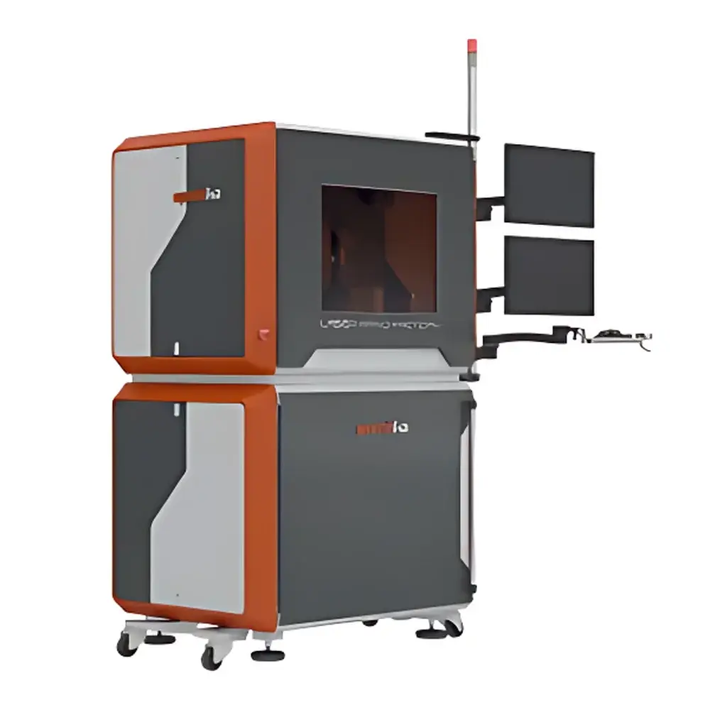
Femtika Laser Nanofactory Integrated Femtosecond Laser Micro/Nano Fabrication System
| Brand | Femtika |
|---|---|
| Origin | Lithuania |
| Manufacturer Type | Original Equipment Manufacturer (OEM) |
| Import Status | Imported |
| Model | Laser Nanofactory |
| Laser Wavelengths | 1028 nm ± 5 nm and 514 nm ± 5 nm |
| Pulse Duration | <290 fs – 10 ps |
| Pulse Energy | >65 µJ |
| Average Power | >4 W |
| Repetition Rate | 60–1000 kHz |
| Cooling | Air-cooled |
| XY Travel Range | 160 mm × 160 mm |
| Z Travel Range | 60 mm |
| Orthogonality | 3 arc sec |
| Positioning Resolution | 1 nm (XY), 2 nm (Z) |
| Max Scan Speed | 350 mm/s (XY), 200 mm/s (Z) |
| Processing Accuracy | <100 nm |
| Compatible Materials | Photonic polymers, fused silica, ceramics, glass, metals |
| Processing Modes | Multiphoton polymerization (MPP), selective laser etching (SLE), direct laser ablation, laser-induced forward transfer (LIFT), subsurface modification |
Overview
The Femtika Laser Nanofactory Integrated Femtosecond Laser Micro/Nano Fabrication System is a high-precision, dual-mode (additive and subtractive) platform engineered for deterministic 3D micro- and nanofabrication across transparent dielectrics, semiconductors, and metals. Unlike conventional two-photon polymerization (TPP) systems limited to photosensitive resins, the Laser Nanofactory leverages ultrashort pulse (<290 fs – 10 ps), high-peak-intensity femtosecond laser irradiation at 1028 nm and frequency-doubled 514 nm wavelengths to induce nonlinear absorption in wide-bandgap materials—including fused silica, sapphire, borosilicate glass, alumina, and stainless steel—enabling true material-agnostic fabrication. Its core operational principle combines multiphoton absorption-driven polymerization with controlled laser-induced defect formation followed by wet or dry selective etching (SLE), as well as direct ablation and subsurface nanograting inscription. This enables simultaneous fabrication of freeform 3D micro-optics, monolithic microfluidic channels, MEMS/NEMS actuators, and hybrid photonic-electronic interfaces—all within a single instrument, without sample relocation or process interruption.
Key Features
- Integrated dual-wavelength femtosecond laser source (1028 nm fundamental + 514 nm SHG) with tunable pulse duration (sub-300 fs to 10 ps), enabling optimization of nonlinear interaction depth and material-specific threshold control.
- High-stability, air-cooled galvo-scanning and precision XYZ nanopositioning stage (1 nm XY / 2 nm Z resolution, 3 arc sec orthogonality) synchronized with real-time beam delivery for sub-100 nm feature fidelity.
- Multi-modal processing architecture supporting seamless switching between multiphoton polymerization (MPP), selective laser etching (SLE), laser ablation, laser-induced forward transfer (LIFT), and subsurface nanograting writing—without hardware reconfiguration.
- Real-time optical feedback integration via coaxial imaging and optional in-situ reflectance/fluorescence monitoring for closed-loop process validation during fabrication.
- Modular vacuum-compatible chamber design accommodating gas-assisted ablation, inert-atmosphere SLE, or ambient processing—ensuring compatibility with ISO Class 5 cleanroom environments and GLP-compliant workflows.
Sample Compatibility & Compliance
The Laser Nanofactory demonstrates validated compatibility with a broad spectrum of functional materials: photonic-grade SU-8, IP-L, and Ormocer® resins; fused silica, BK7, and sapphire substrates; alumina and zirconia ceramics; silicon wafers; and thin-film metallic layers (Au, Ti, Cr, Ni). All fabrication protocols adhere to ASTM F2792 (Standard Terminology for Additive Manufacturing) and ISO/IEC 17025 traceability requirements for dimensional metrology. The system supports full audit trail logging per FDA 21 CFR Part 11 for regulated applications in medical device prototyping and pharmaceutical microdevice development. Process repeatability has been verified across ≥500 consecutive runs under controlled environmental conditions (22 ± 0.5 °C, 45 ± 5% RH), achieving inter-run dimensional deviation ≤±8 nm (3σ) on reference grating structures.
Software & Data Management
Control and workflow orchestration are managed through Femtika’s proprietary NanofabStudio software suite—a modular, Python-extendable platform compliant with IEEE 1516 HLA standards for interoperability. It includes parametric CAD-to-path conversion (supporting STEP, STL, and GDSII imports), physics-based laser-material interaction simulation (using modified Keldysh tunneling models), and automated stitching algorithms for large-area (>10 mm²) structures. All raw scan logs, laser parameter sets, stage trajectories, and metadata are stored in HDF5 format with SHA-256 checksums. Version-controlled project archives support ISO 13485-compliant design history files (DHF), and electronic signatures comply with 21 CFR Part 11 Annex 11 requirements for EU GMP environments.
Applications
- Micro-Optics & Photonics: Fabrication of freeform microlenses, photonic crystal slabs, waveguide couplers, and polarization-selective metasurfaces directly in bulk glass.
- Lab-on-a-Chip & Microfluidics: Monolithic integration of 3D microchannels, valves, mixers, and optical sensing elements into fused silica chips via SLE and MPP hybrid workflows.
- MEMS/NEMS: Direct-write fabrication of suspended cantilevers, resonators, and electrostatic actuators with sub-200 nm gap control and minimal thermal distortion.
- Biosensing & Biointerfaces: Creation of hierarchical surface topographies (e.g., shark-skin mimics, superhydrophobic arrays) on titanium implants and bioactive glass scaffolds for controlled cell adhesion.
- Quantum Device Prototyping: Precision machining of solid-state spin qubit hosts (e.g., NV centers in diamond, rare-earth dopants in YAG) using defect engineering with spatially resolved fluence control.
FAQ
What laser safety class does the Laser Nanofactory operate under?
The system is certified as Class 4 laser product per IEC 60825-1:2014 and incorporates interlocked enclosures, beam shutters, and real-time power monitoring compliant with ANSI Z136.1-2022.
Can the system be integrated with external metrology tools such as SEM or AFM?
Yes—standardized API endpoints and TCP/IP communication protocols enable bidirectional synchronization with coordinate measuring machines (CMM), scanning electron microscopes (SEM), and atomic force microscopes (AFM) for in-line verification.
Is process qualification support available for ISO 13485 or GMP environments?
Femtika provides IQ/OQ/PQ documentation packages, including installation checklists, operational boundary mapping, and performance qualification test scripts aligned with ISO 13485:2016 Annex A and EU Annex 15.
Does the system support multi-user role-based access control?
NanofabStudio implements RBAC (Role-Based Access Control) with configurable permissions for operators, engineers, QA auditors, and administrators—including granular control over parameter editing, job execution, and data export rights.
What is the typical lead time for custom optical path configurations (e.g., Bessel beam generation or 4Pi focusing)?
Standard configurations ship within 12 weeks; custom beam shaping modules (e.g., SLM-based adaptive optics, vortex phase plates) require 16–20 weeks from order confirmation, subject to optical alignment validation reports.


