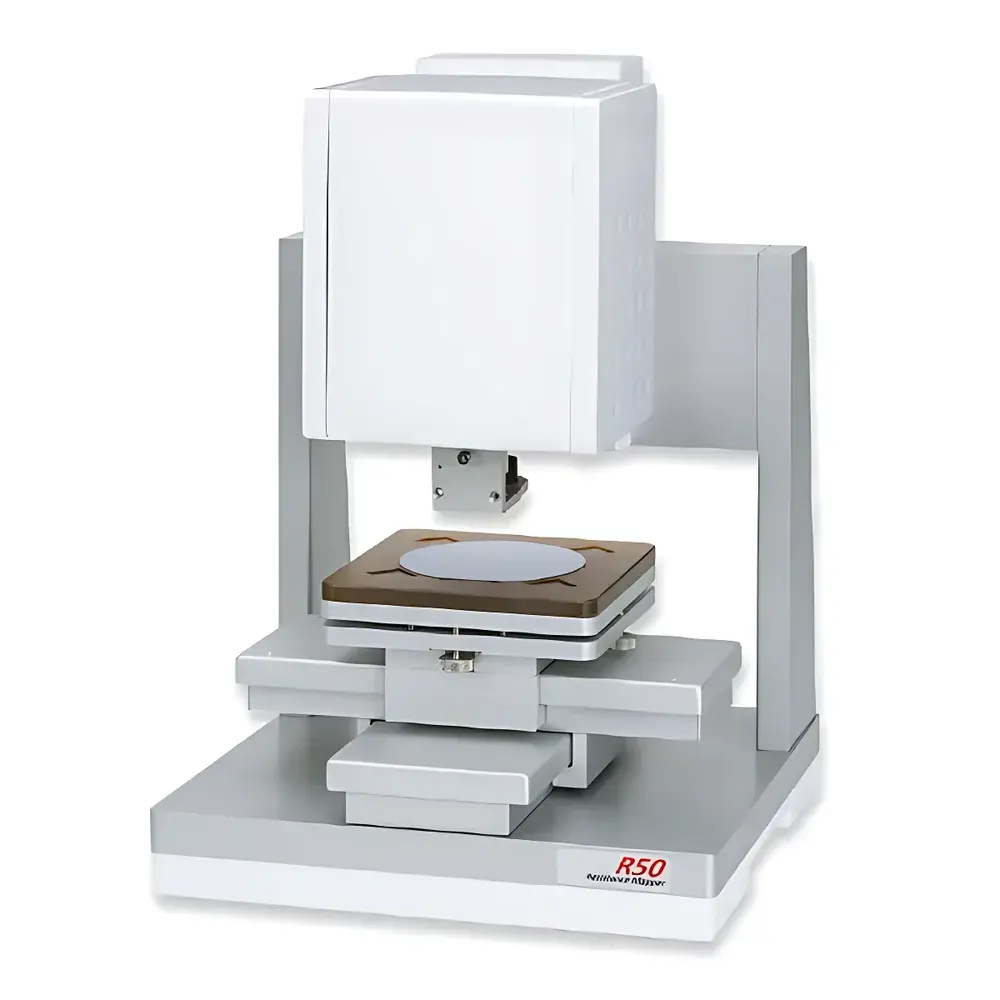
Filmetrics R50 Four-Point Probe Sheet Resistance Mapping System
| Brand | Filmetrics |
|---|---|
| Origin | USA |
| Model | R50 |
| Measurement Principle | Contact Four-Point Probe (4PP) & Non-Contact Eddy Current (EC) |
| Max Sample Diameter | 300 mm |
| Max Mapping Area | 200 mm × 200 mm |
| XY Stage Travel Options | 100 mm × 100 mm or 200 mm × 200 mm (R50-200) |
| Z-Travel | 100 mm |
| Tilt Stage Range | ±5° |
| Mapping Speed | Up to 1 point/sec |
| Software | RsMapper™ with Pattern Generator, GLP-Compliant Data Logging |
Overview
The Filmetrics R50 Four-Point Probe Sheet Resistance Mapping System is an engineered solution for high-throughput, spatially resolved characterization of electrical sheet resistance (Rs) and resistivity (ρ) in conductive and semiconducting thin films. Designed specifically for semiconductor process development, photovoltaic R&D, and advanced display manufacturing, the R50 integrates dual measurement modalities—contact four-point probe (4PP) and non-contact eddy current (EC)—within a single platform. The 4PP method adheres to ASTM F84 and ISO 10700 standards for direct, low-noise DC resistivity quantification, while the EC mode enables rapid, non-destructive evaluation of conductive layers through electromagnetic induction—ideal for fragile, coated, or encapsulated substrates where physical contact is undesirable or prohibited. Its modular architecture supports both inline QA/QC workflows and offline lab-based metrology, delivering traceable, reproducible measurements across wafers up to 300 mm in diameter.
Key Features
- Dual-mode operation: Simultaneous or independent selection of contact 4PP and non-contact eddy current measurement—enabling cross-validation and application-specific optimization.
- Programmable motorized X-Y stage with configurable travel options: standard 100 mm × 100 mm or extended 200 mm × 200 mm (R50-200 variant), supporting full-field mapping of 200 mm × 200 mm areas at ≤1 second per data point.
- Z-axis precision positioning (100 mm travel) and ±5° tilt-adjustable stage for optimized probe alignment on warped or beveled substrates—critical for compound semiconductor and MEMS fabrication.
- RsMapper™ software suite with embedded pattern generator: enables creation of custom measurement grids—including radial, rectangular, circular, or user-defined spot arrays—with exclusion zones, edge masking, and center-aligned sampling logic.
- GLP-compliant data management: timestamped, operator-tagged measurement logs; exportable CSV/Excel reports; audit trail support for FDA 21 CFR Part 11–aligned environments when deployed with validated system configurations.
Sample Compatibility & Compliance
The R50 accommodates rigid and semi-rigid planar substrates including silicon, sapphire, glass, and flexible polymer foils (with appropriate fixturing). It supports doped Si, ITO, AZO, graphene, metal thin films (Al, Cu, TiN), and emerging 2D materials. All contact probes meet SEMI S2/S8 safety requirements and are calibrated per NIST-traceable protocols. The system complies with IEC 61000-6-3 (EMC emissions) and IEC 61010-1 (electrical safety). For regulated environments, optional IQ/OQ documentation packages and electronic signature modules are available to support GMP/GLP validation.
Software & Data Management
RsMapper™ provides full instrument control, real-time visualization of Rs maps, statistical overlay (e.g., σ, min/max, uniformity %), and batch processing of multi-wafer datasets. Maps are exportable as georeferenced TIFF or PNG with embedded metadata (date, operator, probe type, calibration ID). Raw voltage/current readings, temperature compensation logs, and stage position coordinates are stored in structured SQLite databases. Integration with LabVIEW, Python (via PyVISA), and MATLAB is supported through documented API endpoints—facilitating automation within factory MES or academic data pipelines.
Applications
- Semiconductor process monitoring: In-line Rs uniformity assessment of ion-implanted, annealed, or CVD-deposited layers across 200 mm and 300 mm wafers.
- Photovoltaic R&D: Quantifying lateral conductivity gradients in transparent conductive oxides (TCOs) and back-contact metallization stacks.
- Flexible electronics: Non-contact EC mapping of printed silver nanowire or carbon nanotube networks on PET substrates without mechanical stress.
- Research laboratories: Correlating doping concentration profiles with Hall effect data; validating epitaxial layer homogeneity prior to device fabrication.
- Quality assurance: Pass/fail threshold mapping against customer-specified Rs windows (e.g., 10–25 Ω/□ for touch sensor ITO).
FAQ
What standards does the R50 comply with for sheet resistance measurement?
ASTM F84 (Standard Test Method for Measuring Resistivity of Silicon Wafers), ISO 10700 (Electrical resistivity of semiconductor materials), and SEMI MF1530 (Test Method for Sheet Resistance of Semiconductor Wafers Using Four-Point Probes).
Can the R50 measure through passivation layers or thin dielectrics?
Yes—the eddy current mode enables non-contact Rs measurement through dielectric layers up to ~1 µm thick (e.g., SiO₂, SiNx), provided the underlying conductor is sufficiently conductive (>103 S/m) and the frequency sweep is optimized for layer stack impedance.
Is RsMapper software compatible with Windows 11 and 64-bit architectures?
Yes—RsMapper v4.2+ supports Windows 10 and 11 (64-bit only); requires .NET Framework 4.8 and minimum 8 GB RAM for full map rendering of >10,000-point datasets.
Does the system support automated calibration routines?
Yes—built-in reference resistor verification (100 Ω, 1 kΩ, 10 kΩ) with auto-compensation for lead resistance and thermal EMF drift; calibration certificates include uncertainty budgets per ISO/IEC 17025 guidelines.
Can third-party probes be integrated with the R50 platform?
Only Filmetrics-certified 4PP and EC probes are supported for guaranteed accuracy and software interoperability; non-OEM probes void warranty and invalidate compliance documentation.


