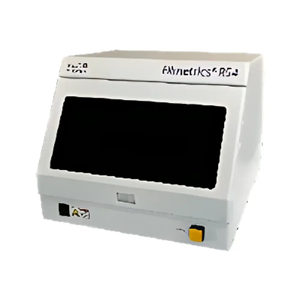
Filmetrics® R54-200/300-4PP/EC Advanced Sheet Resistance Mapping System
| Brand | KLA |
|---|---|
| Origin | USA |
| Manufacturer | KLA Corporation |
| Product Type | Imported Semiconductor Process Metrology Instrument |
| Automation Level | Fully Automated |
| Probe Configurations | Four-Point Probe (4PP) and Eddy Current (EC) |
| Maximum Sample Diameter | 200 mm (R54-200) or 300 mm (R54-300) |
| Maximum Sample Height | 15 mm |
| Sheet Resistance Range | 10⁻² to 10⁸ Ω/sq |
| Measurement Coordinate Modes | Rectangular, Linear, Polar, Custom Grid |
| XY Stage Precision | High-resolution motorized stage with ±100 mm travel (200 mm total range) |
| Enclosed Chamber | Yes, for light- and environment-sensitive samples |
| Software Platform | RSMapper™ v5.x with GLP-compliant audit trail, 21 CFR Part 11 optional modules |
| Compliance | ASTM F84, ISO 10777, SEMI MF67, USP <1054>, supports GMP/GLP documentation workflows |
Overview
The Filmetrics® R54-200/300-4PP/EC Advanced Sheet Resistance Mapping System is a fully automated, dual-mode metrology platform engineered by KLA for high-precision spatial characterization of conductive thin films in semiconductor fabrication, advanced packaging, and emerging flexible electronics processes. Leveraging over 45 years of proprietary four-point probe (4PP) and eddy current (EC) measurement expertise, the R54 integrates contact and non-contact methodologies within a single, enclosed chamber architecture—enabling traceable, reproducible sheet resistance (Rs) and conductivity mapping across wafers up to 300 mm in diameter. Its core measurement principles are grounded in established physical models: the 4PP method applies controlled current through outer probes and measures voltage drop across inner probes to compute Rs under the condition that film thickness is less than half the probe spacing; the EC mode employs high-frequency magnetic induction (10 MHz or 5 MHz coil variants) to generate surface eddy currents, whose amplitude-phase response correlates directly with Rs independent of surface oxidation or mechanical compliance. This dual-sensor architecture eliminates method-dependent bias and supports cross-validated process control in high-mix, high-volume manufacturing environments.
Key Features
- Fully automated operation with programmable recipe-driven mapping sequences and real-time feedback control
- Enclosed, inert-environment-compatible chamber for photolabile, hygroscopic, or air-sensitive samples (e.g., perovskite layers, organic semiconductors)
- Dual-probe capability: interchangeable 4PP and EC modules mounted on a common Z-axis actuator with dynamic height compensation
- High-fidelity XY stage with ±100 mm travel (200 mm total), sub-micron repeatability, and integrated encoder-based position verification
- 10-decade sheet resistance coverage (10⁻²–10⁸ Ω/sq) achieved via optimized probe geometries and adaptive signal conditioning
- Multi-coordinate sampling: rectangular raster, linear scan, polar grid, and user-defined point lists for process-specific layout alignment
- Industry-smallest EC spot size (1.5 mm coil diameter) enabling high-resolution mapping of localized features such as laser-annealed zones or ion-implanted stripes
- KLA-certified probe library including nine 4PP configurations (A–I) and two EC coils (A/B), each calibrated per ASTM F84 Annex B and traceable to NIST standards
Sample Compatibility & Compliance
The R54 accommodates rigid and semi-flexible substrates—including silicon, sapphire, glass, polyimide, and metal foils—with diameters up to 300 mm and heights up to 15 mm. It supports both planar and slightly warped wafers (up to 50 µm TTV) via active Z-height tracking. All measurement protocols adhere to international semiconductor metrology standards: ASTM F84 (Standard Test Method for Measuring Resistivity of Silicon Wafers), ISO 10777 (Electrical characterization of thin conductive films), and SEMI MF67 (Sheet resistance measurements using four-point probe). Optional 21 CFR Part 11-compliant software modules provide electronic signatures, role-based access control, and immutable audit trails required for FDA-regulated R&D and production environments. The system is validated for use in ISO Class 5 cleanrooms and supports integration into factory automation frameworks (SECS/GEM, PV2).
Software & Data Management
RSMapper™ software serves as the unified interface for acquisition, visualization, and statistical analysis. It delivers real-time 2D heatmaps and rotatable 3D topographic plots synchronized with coordinate metadata. Users can overlay multiple parameters (Rs, calculated thickness, resistivity, % uniformity) on a single wafer map and export annotated reports in PDF, CSV, or XML formats compliant with SPC (Statistical Process Control) requirements. Advanced functions include I-V curve generation for leakage detection, radial/diametral profile extraction, edge exclusion masking, and batch-to-batch delta analysis. Data integrity is enforced via built-in calibration logging, probe wear monitoring, and automatic drift correction based on reference standard measurements. All raw data files are stored in vendor-neutral HDF5 format with embedded metadata tags for long-term archival and third-party tool interoperability.
Applications
- Semiconductor front-end: Ion implant dose uniformity mapping, rapid thermal anneal (RTA) optimization, metal silicide formation monitoring, and epitaxial layer resistivity profiling
- Advanced packaging: Redistribution layer (RDL) copper uniformity, bump under-bump metallization (UBM) integrity, and fan-out wafer-level packaging (FOWLP) conductor continuity
- Power devices: SiC and GaN epi-layer sheet resistance homogeneity assessment prior to device isolation
- Flexible electronics: PEDOT:PSS, silver nanowire, and graphene film conductivity mapping on PET and PI substrates
- Photovoltaics: Transparent conductive oxide (TCO) layer uniformity on CIGS and perovskite solar cells
- Battery R&D: Current collector coating uniformity (Al/Cu foils), solid-state electrolyte interfacial resistance screening
- Academic research: Correlation studies between doping concentration, mobility, and Rs in 2D materials and quantum well heterostructures
FAQ
What is the difference between four-point probe and eddy current measurement modes?
Four-point probe provides direct, absolute Rs values with minimal assumptions but requires physical contact and is sensitive to surface contamination or softness. Eddy current offers non-contact, oxide-insensitive measurement ideal for delicate or oxidized films, though it requires empirical calibration for optimal accuracy.
Can the R54 measure ultra-thin (<5 nm) metallic films?
Yes—using high-sensitivity 4PP probes (e.g., Model 610-0591 or 610-0596) with 0.635 mm spacing and low-force loading (≤10 g), the R54 achieves reliable Rs quantification down to sub-1 nm equivalent thicknesses when combined with material-specific resistivity inputs.
How does the system handle wafer warpage during mapping?
The integrated capacitive Z-sensor continuously monitors sample height at each measurement point and dynamically adjusts probe standoff distance, ensuring consistent contact force (4PP) or lift-off (EC) across full-wafer scans.
Is RSMapper compatible with existing MES or SPARK systems?
Yes—RSMapper supports OPC UA and RESTful API interfaces for seamless integration with Manufacturing Execution Systems (MES), Statistical Process Control (SPC) platforms, and yield management dashboards.
Does KLA provide NIST-traceable calibration services?
KLA offers annual on-site calibration and certification services aligned with ISO/IEC 17025, including uncertainty budgets per probe type and frequency band, with full documentation for internal QA and external audit readiness.


