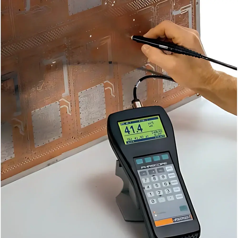
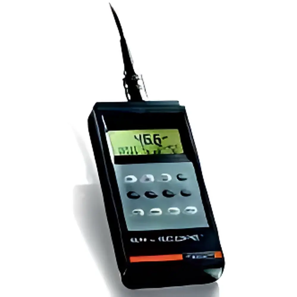
FISCHER PMP10 Copper Thickness Gauge
| Origin | Germany |
|---|---|
| Manufacturer Type | Authorized Distributor |
| Origin Category | Imported |
| Model | PMP10 |
| Pricing | Upon Request |
Overview
The FISCHER PMP10 Copper Thickness Gauge is a precision handheld eddy current-based instrument engineered for non-destructive measurement of conductive copper layers on non-conductive or weakly conductive substrates—particularly optimized for printed circuit board (PCB) manufacturing and quality assurance. Unlike optical or mechanical methods, the PMP10 employs phase-sensitive high-frequency eddy current technology (operating at 60 kHz and 240 kHz selectable frequencies), enabling accurate determination of copper thickness in challenging geometries: within plated through-holes (PTH), beneath solder mask (S/M), on surface traces, and across copper foil laminates. Its design adheres to the physical principles defined in ASTM B567 (Standard Test Method for Measurement of Coating Thickness by the Eddy Current Method) and supports traceable calibration per ISO/IEC 17025 requirements when used with certified reference standards. The device is not intended for standalone metrology lab use but serves as an integrated field verification tool aligned with IPC-6012, IPC-4552A (for ENIG/ENEPIG), and IPC-TM-650 2.2.13 test methodologies.
Key Features
- Phase-resolved eddy current sensing with dual-frequency capability (60 kHz / 240 kHz) for optimized resolution across thin (100 µm) copper deposits
- Dedicated probe configurations: ESD20ZN (for rough-surface Zn/Cu/Al on steel), ESD2.4 (micro-area Zn on small ferrous parts), ESD20NI (Ni plating on steel, frequency-selective mode)
- Non-destructive measurement of copper wall thickness inside drilled vias (≥0.2 mm diameter) without sectioning or microsectioning
- Direct measurement of copper thickness under solder mask—no mask removal required—validated against cross-sectional SEM correlation studies
- Automatic substrate recognition logic minimizes operator-induced error; no manual zeroing needed for common FR-4, polyimide, or ceramic substrates
- Ruggedized industrial housing rated IP54; operating temperature range: 10–40 °C; relative humidity ≤80% non-condensing
Sample Compatibility & Compliance
The PMP10 is validated for use on rigid and flexible PCBs, copper-clad laminates (CCL), and electroplated metal components where copper serves as functional conductor or barrier layer. It accommodates substrates including FR-4, BT resin, polyimide, alumina, and glass. Measurement validity requires substrate conductivity < 10−6 S/m and dielectric constant εr < 5.0. The instrument complies with electromagnetic compatibility (EMC) directive 2014/30/EU and low-voltage directive 2014/35/EU. While not FDA-cleared, its measurement data supports GLP/GMP documentation workflows when paired with Fischer’s optional audit-trail-enabled software (see Software & Data Management). Calibration certificates are issued per DIN EN ISO 17025 by accredited third-party labs upon request.
Software & Data Management
The PMP10 operates autonomously but integrates via USB or Bluetooth with FISCHER’s FISCHER DataCenter v4.x software suite. This platform enables batch export of measurement series (CSV, XML), statistical process control (SPC) charting (X̄-R, Cpk), and automated report generation compliant with IPC-A-600 and IPC-6012 documentation templates. All user actions—including probe changes, calibration events, and parameter edits—are time-stamped and logged with operator ID, satisfying 21 CFR Part 11 electronic record/electronic signature (ER/ES) requirements when configured with role-based access control and digital certificate authentication.
Applications
- Verification of inner-layer and outer-layer copper thickness pre- and post-etch in HDI and multilayer PCB fabrication
- In-process monitoring of PTH copper wall thickness during electroplating line qualification and maintenance
- Final QA inspection of copper foil adhesion and uniformity on flexible circuits (flex-rigid hybrids)
- Thickness validation of copper seed layers in advanced packaging (e.g., fan-out wafer-level packaging FO-WLP)
- Coating thickness auditing for copper diffusion barriers (e.g., Ta/TaN) in semiconductor interconnect stacks
- Supplier qualification testing for copper-clad laminates per IPC-4101D specifications
FAQ
Can the PMP10 measure copper thickness on aluminum substrates?
No—the eddy current method requires a non-conductive or magnetically permeable base material; aluminum is highly conductive and causes signal interference. Use XRF-based instruments (e.g., FISCHER XDV-SDD) for Cu/Al systems.
Is probe recalibration required when switching between via-wall and surface-copper measurements?
No—probe-specific calibration curves are stored internally; the instrument auto-selects the appropriate algorithm based on probe ID and measurement mode.
Does the PMP10 support statistical process control (SPC) output?
Yes—when connected to FISCHER DataCenter, it exports full SPC-ready datasets including mean, standard deviation, Cp/Cpk, and trend charts.
What is the minimum via diameter measurable with the standard PTH probe?
0.2 mm internal diameter, assuming ≥15° via wall angle and ≥25 µm nominal copper thickness.
Can measurement data be exported to MES or ERP systems?
Yes—via CSV/XML API integration or OPC UA gateway modules available through Fischer’s Industrial Connectivity Package.


