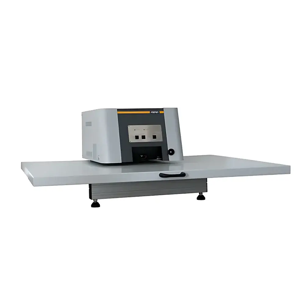
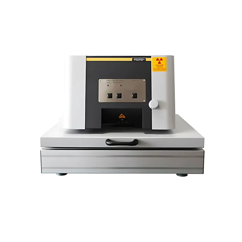
Fischer XDLM-PCB X-ray Fluorescence Coating Thickness Analyzer for Gold and Nickel Plating
| Origin | Germany |
|---|---|
| Manufacturer Type | Authorized Distributor |
| Origin Category | Imported |
| Model | XDLM-PCB |
| Pricing | Available Upon Request |
Overview
The Fischer XDLM-PCB is a benchtop energy-dispersive X-ray fluorescence (EDXRF) analyzer engineered for non-destructive, high-precision measurement of thin metallic coatings—specifically gold and nickel—on printed circuit boards (PCBs) and other micro-structured electronic components. Operating on the fundamental principle of characteristic X-ray emission, the instrument irradiates the sample with a focused X-ray beam; emitted fluorescent radiation is spectrally resolved to quantify elemental composition and calculate coating thickness via fundamental parameter (FP) algorithms. Its design centers on metrological reliability in production-critical environments: the integrated laser alignment system ensures repeatable sample positioning, while the drawer-style sample chamber with bottom-slot access enables rapid, operator-safe loading of PCBs up to standard industry dimensions. The system complies with ISO 3497 (Metallic coatings — Measurement of coating thickness — X-ray spectrometric methods) and supports traceable calibration per ASTM B568 and DIN EN ISO 3497.
Key Features
- Micro-focused tungsten X-ray tube with beryllium window, delivering stable excitation across three selectable high-voltage settings (30 kV, 40 kV, 50 kV) optimized for light-to-heavy element detection.
- Patented Distance Compensation Method (DCM) enabling accurate thickness quantification over variable measurement distances from 0 mm to 10 mm—critical for warped or uneven PCB substrates.
- 0.2 mm collimator aperture yielding a minimum spot size of ~0.16 mm at nominal working distance, visualized in real time via integrated high-resolution video camera.
- Dual-mode operation: simultaneous multi-element analysis (up to 24 elements) and single-layer or multi-layer coating thickness determination (e.g., Ni under Au, Cu under Ni).
- Robust mechanical architecture with vibration-damped optical path and temperature-stabilized detector electronics to ensure long-term measurement reproducibility (RSD < 2% for 100 nm Au on Ni).
Sample Compatibility & Compliance
The XDLM-PCB accommodates rigid and flexible PCBs, connector pins, lead frames, and small-volume electroplated components with maximum dimensions of 300 × 300 mm and height ≤ 50 mm. It supports direct analysis of solder masks, silkscreen, and surface finishes without sample preparation. Regulatory compliance includes full alignment with EU RoHS Directive 2011/65/EU for restricted substance screening (Pb, Cd, Hg, Cr⁶⁺, Br), as well as support for GLP/GMP documentation workflows—including audit trails, user access levels, and electronic signatures compliant with FDA 21 CFR Part 11 when integrated with Fischer’s WinFTM® software.
Software & Data Management
Controlled by WinFTM® Professional software, the system provides intuitive method setup, automated batch measurement sequencing, and statistical process control (SPC) reporting. All spectra, measurement parameters, and calibration files are stored in a secure SQLite database with timestamped metadata. Export formats include CSV, PDF reports (with embedded spectra), and XML for LIMS integration. Software validation packages (IQ/OQ/PQ documentation) are available to support regulated manufacturing environments in automotive (IATF 16949), medical device (ISO 13485), and semiconductor (SEMI S2/S8) sectors.
Applications
- Quality assurance of immersion gold (ENIG) and electroless nickel immersion gold (ENEPIG) finishes on PCBs.
- Thickness verification of nickel barrier layers beneath gold contacts in RF connectors and high-frequency interconnects.
- Process monitoring of selective plating lines for semiconductor packaging substrates.
- Material verification of precious metal content in watch components, eyewear hinges, and automotive sensor housings.
- Failure analysis of delamination or insufficient underplate thickness leading to solder joint brittleness or corrosion susceptibility.
FAQ
What is the minimum detectable thickness for gold on nickel using the XDLM-PCB?
Detection limits depend on measurement time, geometry, and substrate composition; typical lower limits are ~0.01 µm for Au on Ni with 60 s acquisition.
Can the instrument measure multi-layer stacks such as Cu/Ni/Au?
Yes—it supports quantitative analysis of up to three consecutive layers using FP modeling with matrix correction.
Is helium purge required for light element analysis?
No—air-path operation suffices for Cl–U elements; optional He purge accessory enables enhanced sensitivity for Na–Cl range if needed.
How is calibration maintained across different operators and shifts?
Calibration is stored per method; built-in drift correction uses internal reference standards and periodic verification checks against certified reference materials (CRMs).


")