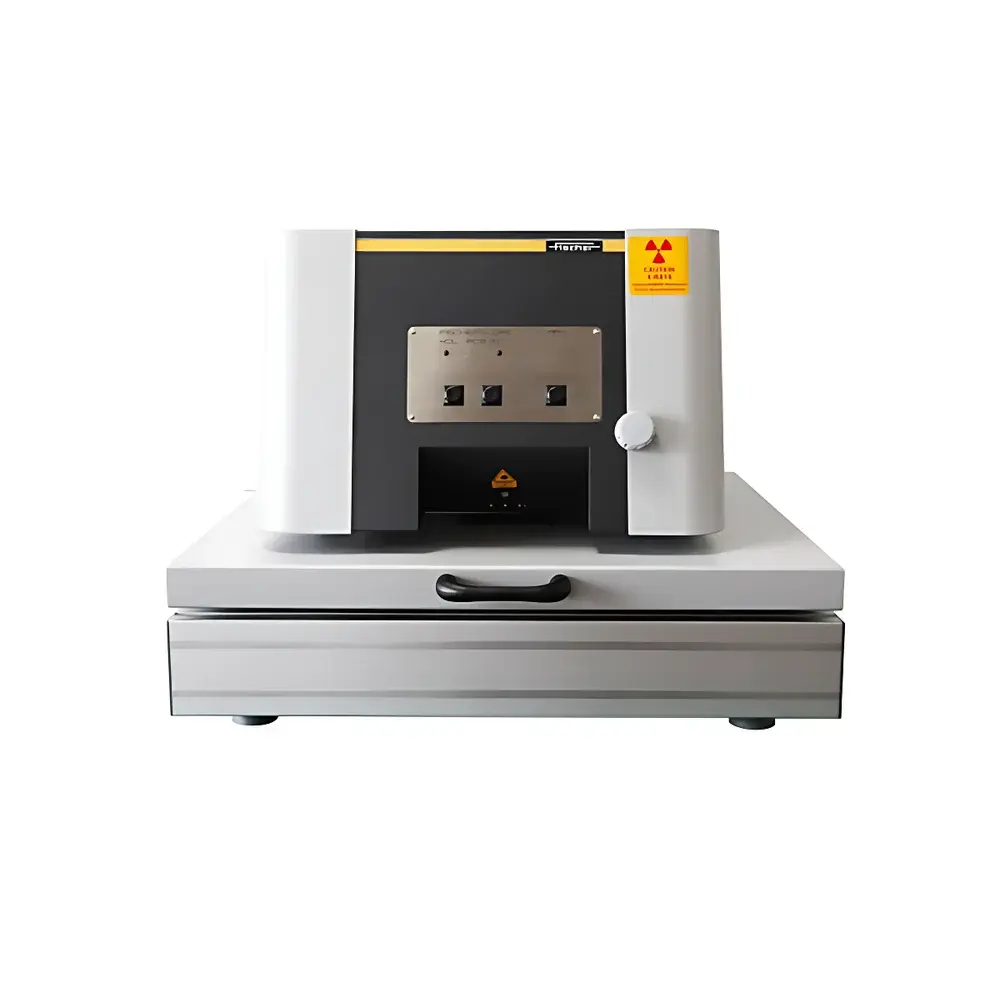
Fischer XDLM-PCB Series X-ray Fluorescence Thickness Analyzer
| Origin | Guangdong, China |
|---|---|
| Manufacturer Type | Authorized Distributor |
| Origin Classification | Domestic (China) |
| Model | Fischer XDLM-PCB 200 / 210 / 220 |
| Price Range | USD 70,000 – 140,000 |
Overview
The Fischer XDLM-PCB Series is a benchtop energy-dispersive X-ray fluorescence (EDXRF) thickness analyzer engineered for non-destructive, quantitative measurement of metallic coating thicknesses and elemental composition on printed circuit boards (PCBs). Utilizing fundamental parameter (FP) algorithms and calibrated spectral deconvolution, the system determines layer thicknesses—such as Au/Ni/Cu/Sn/Pd on Cu substrates—by analyzing characteristic X-ray intensities emitted under controlled Rh or Mo anode excitation. Designed specifically for electronics manufacturing quality control, it delivers traceable, repeatable results in production-line and laboratory environments without sample preparation or contact. Its optical geometry, fixed high-resolution detector, and integrated collimation ensure stable performance across multilayer stack configurations typical in HDI and fine-pitch PCBs.
Key Features
- Three platform variants: XDLM-PCB 200 (manual drawer-style sample loading with integrated laser crosshair), XDLM-PCB 210 (motorized XY stage with programmable positioning and auto-eject function), and XDLM-PCB 220 (enhanced XY stage with higher positional repeatability ±1 µm and optional Z-height sensing)
- High-resolution color CCD camera (1.3 MP, real-time magnification up to 40×) co-registered with X-ray beam path for precise visual alignment of measurement spots on solder pads, bond fingers, and ENIG/ENEPIG surfaces
- Optimized EDXRF optics including selectable primary beam filters, Peltier-cooled silicon drift detector (SDD) with <135 eV Mn Kα resolution, and collimators down to 30 µm diameter for micro-area analysis
- Rh or Mo X-ray tube (50 kV / 1 mA max) with automatic kV/mA optimization per layer stack to maximize signal-to-background ratio and minimize matrix effects
- Robust mechanical architecture with vibration-dampened baseplate and temperature-stabilized chamber, enabling stable operation over extended shifts in ambient lab conditions (20–25 °C, 40–60% RH)
Sample Compatibility & Compliance
The XDLM-PCB series accommodates standard PCB formats up to 300 × 300 mm (XDLM-PCB 210/220) or 200 × 200 mm (XDLM-PCB 200), with Z-clearance up to 80 mm for tall components. It supports single-layer, dual-layer (e.g., Ni/Au), and triple-layer (e.g., Cu/Ni/Au) systems on FR-4, polyimide, and ceramic substrates. Measurement uncertainty complies with DIN ISO 3497:2022 (Metallic coatings — Measurement of coating thickness — X-ray spectrometric methods) and ASTM B568-17 (Standard Test Method for Thickness Measurement of Metallic Coatings by X-Ray Spectrometry). System validation includes certified reference materials (CRMs) traceable to NIST and PTB, and full audit trails support GLP/GMP documentation requirements.
Software & Data Management
WINFTM® software (v6.5+, Windows 10/11 64-bit) provides full instrument control, method development, and statistical reporting. Key capabilities include multi-point mapping routines with CSV/Excel export, SPC charting (X̄/R, Cpk), batch measurement scripting, and customizable report templates compliant with internal QA protocols. All raw spectra, calibration files, and user actions are logged with timestamped metadata. The software supports FDA 21 CFR Part 11 compliance through electronic signatures, role-based access control, and immutable audit trails—enabling use in regulated electronics manufacturing facilities subject to ISO 9001 and IATF 16949 audits.
Applications
- Quantitative thickness verification of electroless nickel immersion gold (ENIG), electroless nickel electroless palladium immersion gold (ENEPIG), and immersion tin/silver coatings on PCB final finishes
- Process monitoring of plating bath stability via periodic Ni/Au thickness ratio tracking and intermetallic phase detection (e.g., Ni₃Sn₄ at Cu/Sn interfaces)
- Failure analysis of solder joint reliability issues linked to insufficient Ni barrier thickness or Au embrittlement
- Supplier qualification testing per IPC-4552B (ENIG) and IPC-4556 (ENEPIG) specifications
- Inline QC station integration via Ethernet/IP or Modbus TCP for MES data exchange
FAQ
What coating systems can be measured with the XDLM-PCB series?
Au, Ni, Pd, Sn, Ag, Cu, and Cr layers on Cu, brass, or alloy substrates—up to three consecutive layers—with thickness ranges from 0.01 µm (Au) to 50 µm (Ni), depending on matrix and excitation conditions.
Is helium purge required for light element analysis?
No—air-path measurement suffices for Ni, Cu, and heavier elements; optional He purging is available for enhanced sensitivity to P and S in organic contamination studies.
How is calibration maintained across production shifts?
Daily verification using on-board CRMs and automated drift correction via internal reference peaks ensures long-term calibration stability; full recalibration is recommended every 6 months or after hardware service.
Can the system measure through solder mask?
Yes—provided the mask is non-halogenated and ≤30 µm thick; spectral interference must be evaluated case-by-case using FP modeling in WINFTM®.
Does the instrument require external cooling or compressed air?
No—integrated thermoelectric cooling and passive heat dissipation eliminate need for chillers or air lines, reducing facility infrastructure requirements.


