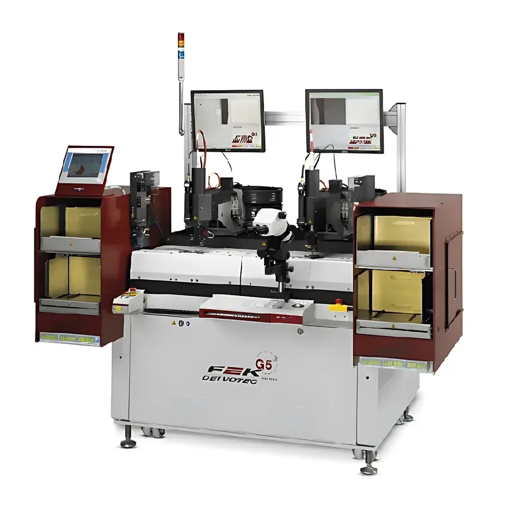
F&K ACCμRA OPTO Flip-Chip Bonder (G5/2017 Series)
| Brand | SET/Sensor Electronic Technology |
|---|---|
| Origin | Germany |
| Model | G5/2017 Series |
| Bonding Accuracy | ±0.5 µm |
| Bonding Methods | Thermocompression, Reflow Soldering, UV Curing |
| Compatible Materials | Au, Au/Sn, In, Cu, Cu/Sn |
| Applications | Flip-Chip, Die-to-Substrate (D2S), Chip-to-Chip (C2C), Chip-to-Substrate (C2S), MEMS, MOEMS, MCM, Photonic Integrated Circuits (PICs), Silicon Photonics, Optoelectronic Assembly |
Overview
The F&K ACCμRA OPTO Flip-Chip Bonder (G5/2017 Series) is a high-precision, semi-automated thermocompression and reflow bonding platform engineered for advanced optoelectronic and silicon photonic packaging. Developed by F&K Delvotec Bondtechnik and distributed globally by SET (Sensor Electronic Technology), this system implements a closed-loop motorized motion architecture with sub-micron positional repeatability—specifically calibrated to ±0.5 µm in X/Y/Z alignment under controlled thermal and force conditions. Its core operational principle integrates real-time vision-based die placement, programmable thermal profiling (up to 400 °C), and dynamic force control (0.1–100 cN range) to enable low-force, high-fidelity interconnect formation without die cracking or substrate warpage. Designed explicitly for R&D and low-to-medium volume production environments, the ACCμRA OPTO supports both bumpless and micro-bumped die attach, making it suitable for heterogeneous integration of III–V devices onto silicon interposers, hybrid PIC assembly, and wafer-level optical alignment tasks.
Key Features
- Motorized precision stages with integrated linear encoders and active vibration damping for ±0.5 µm placement accuracy and <0.3 µm repeatability over extended operation cycles
- Dual-vision system: Top-side telecentric optics (5×–50× magnification) and bottom-side IR-transparent imaging for simultaneous top/bottom alignment of transparent or opaque substrates
- Programmable thermocompression module with dual-zone heating (substrate + capillary/tool), ramp rates from 0.1 to 10 °C/s, and temperature stability of ±0.5 °C at setpoint
- Multi-process capability: Supports thermocompression bonding, reflow soldering (with inert N₂ or formic acid ambient), and UV-curable adhesive dispensing & curing (365 nm LED source, 0–5 W/cm² intensity)
- Modular tooling interface compatible with standard capillaries (e.g., 100–500 µm ID), custom bond tools, and vacuum pick-up nozzles for fragile dies (e.g., InP, GaAs, LiNbO₃)
- Open software architecture with Ethernet/IP and SECS/GEM protocol support for integration into factory automation systems and MES environments
Sample Compatibility & Compliance
The ACCμRA OPTO accommodates substrates up to 200 mm × 200 mm (customizable to 300 mm), including silicon, glass, quartz, alumina, and flexible polyimide carriers. It handles die sizes from 50 µm × 50 µm to 20 mm × 20 mm, with thicknesses ranging from 50 µm to 1.5 mm. The system complies with IEC 61000-6-2 (EMC immunity) and IEC 61000-6-4 (EMC emissions), and meets CE safety directives (2014/30/EU, 2014/35/EU). For regulated environments, optional audit trail logging, electronic signature support, and 21 CFR Part 11–compliant data archiving modules are available—enabling alignment with GLP, ISO 9001:2015, and JEDEC J-STD-020D moisture sensitivity level (MSL) handling protocols.
Software & Data Management
Operation is managed via the proprietary BondWare™ v5.x control suite, featuring a deterministic real-time kernel (Linux PREEMPT_RT) and intuitive graphical workflow editor. Each bonding sequence stores full metadata—including thermal profiles, applied force curves, vision alignment residuals, and environmental logs (temperature, humidity, N₂ flow)—in SQLite3 databases with SHA-256 hash integrity verification. Raw image files (TIFF/16-bit) and process parameter sets are exportable in ASTM E2658-compliant XML format. Optional cloud synchronization enables remote diagnostics, version-controlled recipe sharing across global R&D sites, and automated SPC chart generation for Cp/Cpk trending per bond site.
Applications
- Silicon photonics: Edge coupling alignment of laser diodes and modulators onto SOI waveguides
- Photonic integrated circuits (PICs): Heterogeneous integration of InP gain sections with SiN passive circuits
- MEMS/MOEMS packaging: Hermetic die attach of scanning mirrors and optical switches using Au–Sn eutectic
- High-speed optoelectronics: C2C bonding of VCSEL arrays to driver ICs with <10 µm pitch tolerance
- Advanced sensing: Low-stress attachment of thin-film piezoresistive sensors onto flexible substrates
- Quantum device assembly: Cryogenic-compatible flip-chip interconnects for superconducting qubit readout lines
FAQ
What types of bonding processes does the ACCμRA OPTO support?
Thermocompression, reflow soldering (with controlled atmosphere options), and UV-curable adhesive bonding.
Is the system compatible with bumpless die attach?
Yes—it supports direct metal-to-metal bonding (e.g., Cu–Cu, Au–Au) without pre-deposited bumps, leveraging surface activation and atomic diffusion under controlled T/F conditions.
Can it handle fragile compound semiconductor dies?
Yes—its low-force actuation (<0.5 cN minimum resolution) and vacuum-assisted pickup prevent chipping or fracture of InP, GaAs, or LiNbO₃ dies.
Does it support automated recipe transfer between R&D and pilot-line environments?
Yes—BondWare™ enables binary recipe portability, with configurable process lock-down levels for operator privilege management and change control compliance.
What documentation packages are provided for qualification in regulated industries?
IQ/OQ/PQ protocols, traceable calibration certificates (DKD-accredited), FAT/SAT reports, and URS-aligned validation templates are supplied as part of the delivery package.


