FRT FRT Optical Surface Metrology System
| Brand | FRT |
|---|---|
| Origin | Germany |
| Manufacturer Type | Authorized Distributor |
| Product Category | Imported Instrument |
| Model | FRT Optical Surface Metrology System |
| Pricing | Available Upon Request |
Overview
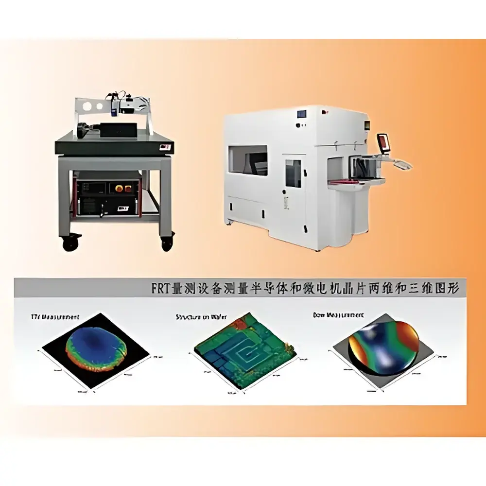
The FRT Optical Surface Metrology System is a high-precision, non-contact optical profiler engineered for nanoscale topographic characterization of flat and slightly curved surfaces. Based on advanced white-light interferometry (WLI) and/or confocal chromatic aberration principles—depending on the selected sensor module—the system delivers traceable, repeatable surface form measurements including Total Thickness Variation (TTV), Bow, and Warp with sub-nanometer vertical resolution. Designed specifically for demanding semiconductor fabrication environments, it supports inline and offline metrology workflows where surface geometry integrity directly impacts lithography overlay accuracy, thin-film uniformity, and wafer-level packaging yield. Its modular architecture enables seamless integration into cleanroom automation frameworks and compatibility with SEMI E10/E11/E30 standards for equipment communication and data exchange.
Key Features
- Non-contact optical measurement—eliminates mechanical loading, surface scratching, or thermal drift artifacts common in stylus profilometers
- Modular sensor platform supporting up to 25 interchangeable optical heads, including wide-field WLI, micro-confocal, and telecentric imaging variants
- Nanometer-level vertical resolution (≤0.1 nm RMS noise floor) and sub-micrometer lateral resolution across measurement fields ranging from 0.1 mm² to >300 mm × 300 mm
- High-speed acquisition: full-wafer TTV/Bow maps completed in under 60 seconds for 200 mm substrates; <5 minutes for 300 mm wafers with full spatial sampling
- Large-format capability: accommodates substrates up to 450 mm diameter and irregularly shaped components (e.g., reticles, optics blanks, MEMS wafers)
- Customizable hardware/software configurations—including vacuum-compatible stages, temperature-stabilized enclosures, and SECS/GEM interface modules—for integration into automated fabs and R&D labs
Sample Compatibility & Compliance
The system supports a broad range of reflective and semi-transparent materials critical to semiconductor manufacturing: silicon, sapphire, SiC, GaN, fused silica, quartz, and patterned wafers with dielectric stacks (e.g., SiO₂/SiN). It complies with ISO 25178-2 (surface texture parameters), ISO 10110-5 (optical component flatness), and ASTM F394 (standard test method for warp and bow of silicon wafers). For regulated environments, optional FDA 21 CFR Part 11-compliant software packages provide electronic signatures, audit trails, and role-based access control—fully aligned with GLP and GMP documentation requirements. All calibration procedures follow NIST-traceable protocols, with annual recalibration supported via FRT-certified service centers in Europe, North America, and Asia.
Software & Data Management
FRT’s proprietary MetroStyler™ software provides a unified interface for instrument control, real-time visualization, and statistical process control (SPC) reporting. It includes automated recipe-driven measurement sequences, multi-layer stack analysis (for film-induced stress evaluation), and GD&T-compliant form deviation mapping (ISO 1101). Raw height data is stored in HDF5 format for long-term archival and interoperability with MATLAB, Python (via h5py), and industry-standard SPC platforms (e.g., InfinityQS, Minitab). The system supports direct export to CSV, STEP AP242, and VDA-FS formats, enabling bidirectional data flow with MES and CIM systems. Optional API access allows integration with factory host systems via RESTful endpoints or OPC UA.
Applications
- Semiconductor front-end: TTV/Bow/Warp verification of polished wafers pre-epitaxy and post-CMP; monitoring of stress-induced deformation during thin-film deposition
- Advanced packaging: warpage analysis of fan-out wafer-level packages (FO-WLP), interposer flatness assessment, and solder bump coplanarity validation
- Optics & photonics: flatness certification of laser cavity mirrors, EUV mask blanks, and AR/HR coating substrates
- MEMS & sensors: release etch-induced curvature quantification, diaphragm deflection profiling, and comb-drive alignment verification
- Materials R&D: anisotropic etch rate mapping, ion implantation damage assessment, and thermal expansion coefficient correlation studies
FAQ
What measurement principles does the FRT Optical Surface Metrology System employ?
It primarily utilizes white-light interferometry (WLI) for high-resolution surface topography and confocal chromatic sensing for steep-slope or transparent-layer applications—sensor selection is configurable per use case.
Can the system measure patterned or structured wafers?
Yes—advanced phase-unwrapping algorithms and multi-scale scanning modes enable accurate form measurement over shallow trenches, alignment marks, and low-contrast metallization layers without requiring masking or averaging.
Is the system compliant with semiconductor fab automation standards?
Yes—SECS/GEM, GEM300, and PV2 interfaces are available as factory-installed options; all communication protocols conform to SEMI E30, E37, and E40 specifications.
How is traceability maintained for calibration and measurement uncertainty?
Each system ships with NIST-traceable step-height and flatness reference artifacts; uncertainty budgets are generated per ISO/IEC 17025 guidelines and documented in the Certificate of Calibration.
What support is provided for regulatory audits in pharmaceutical or medical device manufacturing?
FDA 21 CFR Part 11-compliant software packages include full audit trail logging, electronic signature workflows, and IQ/OQ documentation templates validated per GAMP5 practices.


