Gel-Pak BMP Bumped Die Carrier
| Brand | Gel-Pak |
|---|---|
| Origin | USA |
| Manufacturer Type | Authorized Distributor |
| Import Status | Imported |
| Model | Gel-Pak BMP |
| Price Range | USD 10–14 |
Overview
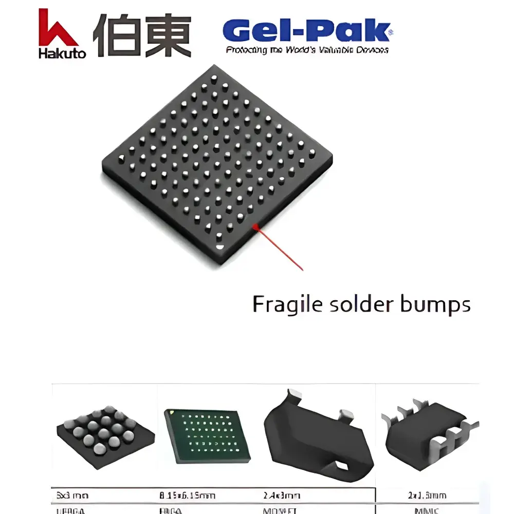
The Gel-Pak BMP (Bumped Die Carrier) is a precision-engineered semiconductor handling solution designed specifically for devices with non-planar surface topographies—such as solder bumps, copper pillars, or micro-balls found on bumped wafers, flip-chip dies, ball grid arrays (BGAs), and discrete power devices like MOSFETs. Unlike conventional flat-surface carriers that rely on uniform vacuum or mechanical clamping, the BMP series employs a proprietary elastomeric gel interface engineered to conform dynamically to protruding features while maintaining controlled, repeatable adhesion force. This contact-adaptive mechanism ensures secure immobilization without compressing or shearing delicate bump structures—a critical requirement in advanced packaging workflows where bump height tolerances fall below 25 µm and coplanarity deviations exceed ±5 µm. The carrier operates within Class 100–Class 10 cleanroom environments and is validated for use in wafer-level testing, die bonding, and automated pick-and-place (PNP) transfer stages.
Key Features
- Conformal Gel Interface: A low-compliance, high-damping silicone-based gel matrix that deforms selectively around individual bumps—maximizing real contact area while minimizing localized stress on solder joints or under-bump metallurgy (UBM).
- JEDEC-Compliant Footprint: Available in standard 2-inch (50.8 mm) and 4-inch (101.6 mm) formats aligned with JEDEC MO-122 and MO-220 outlines, enabling drop-in integration into existing carrier handling systems and FOUP/SMIF loadports.
- Automated Equipment Compatibility: Designed for seamless integration with industry-standard PNP platforms—including ASM Pacific, Mycronic, and Besi pick-and-place tools—via standardized fiducial patterns and edge clearance specifications.
- ESD-Safe Configuration Option: Optional carbon-loaded elastomer formulation meeting ANSI/ESD S20.20 requirements (<1×10⁶ Ω surface resistivity), certified for handling Class 0 (HBM <250 V) electrostatic-sensitive devices.
- Controlled Release Profile: Adhesion force remains stable across temperature ranges of 20–40 °C and relative humidity levels of 30–60% RH, with release torque <0.05 N·mm per 1 mm² bump footprint—enabling reliable, residue-free die detachment.
Sample Compatibility & Compliance
The Gel-Pak BMP carrier accommodates a broad spectrum of non-planar semiconductor components, including but not limited to: bumped silicon dies (e.g., image sensors, RF transceivers), flip-chip packaged ASICs, fine-pitch BGAs (≤0.4 mm pitch), and discrete trench-gate MOSFETs with elevated source pads. All configurations comply with JEDEC J-STD-033 moisture sensitivity level (MSL) handling guidelines when used in conjunction with dry nitrogen storage protocols. The gel material is ISO 14644-1 Class 5 compatible and exhibits no outgassing per ASTM E595, making it suitable for vacuum probe station applications. Traceability is supported via laser-etched lot codes compliant with SEMI E10 standards.
Software & Data Management
While the BMP carrier is a passive mechanical component, its design supports full traceability within Industry 4.0 manufacturing execution systems (MES). Each unit carries a unique serialized QR code linked to a digital twin profile containing material certification (RoHS, REACH), gel lot-specific compression modulus data, and calibration history. When deployed in automated lines, the carrier’s fiducial alignment geometry enables machine vision-based verification per SEMI E142 specifications. Audit trails—including usage cycle count, exposure duration, and cleaning log entries—are maintained in accordance with FDA 21 CFR Part 11–compliant electronic record systems when integrated with MES platforms such as Siemens Opcenter or Applied Materials EnduraTrack.
Applications
- Wafer-level burn-in and electrical testing of bumped die prior to singulation
- High-precision die attach in fan-out wafer-level packaging (FO-WLP) processes
- Automated optical inspection (AOI) of bump coplanarity and solder joint integrity
- Transport between lithography, plating, and reflow stations in advanced packaging fabs
- Reliability qualification testing—including thermal cycling (JESD22-A104) and mechanical shock (JESD22-B104)—where uncontrolled die movement could invalidate failure mode analysis
FAQ
Is the Gel-Pak BMP carrier reusable?
Yes—each unit is rated for ≥500 handling cycles under controlled cleanroom conditions (ISO Class 5), provided proper cleaning per Gel-Pak Technical Bulletin TB-017 is followed.
Can the BMP carrier be sterilized for biomedical device packaging?
No—this product is not gamma- or EtO-sterilizable; it is intended solely for semiconductor fabrication and test environments.
Does the gel interface require periodic replacement?
The elastomeric surface retains functional integrity for ≥12 months when stored at 23 ± 2 °C and protected from UV exposure and hydrocarbon solvents.
What bump heights are supported?
Validated performance range: 25–200 µm bump height with aspect ratios up to 1:3 (height:diameter); extended validation available upon request for pillar structures >300 µm.
How does the BMP carrier compare to vacuum chucks for bump handling?
Unlike vacuum chucks—which risk pulling bumps off the die or inducing tilt due to uneven suction distribution—the BMP relies on distributed viscoelastic contact, eliminating point-load risks and ensuring consistent coplanar registration during placement.
Related Products


