Gel-Pak GEM Series Precision Gel-Based Component Carrier for Semiconductor and Optical Components
No specifications available.
Overview
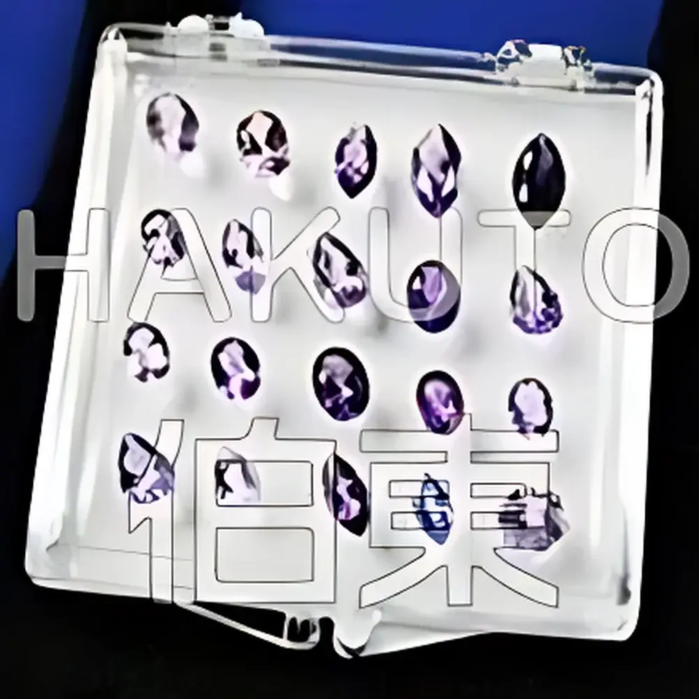
The Gel-Pak GEM Series is a precision-engineered, reusable gel-based component carrier system originally developed for the secure handling and presentation of high-value gemstones and fine jewelry. Its underlying technology—based on proprietary, high-crosslink-density polymer gels—has been rigorously adapted for cleanroom-compatible applications in semiconductor manufacturing, photonics, MEMS, and micro-optical assembly. Unlike conventional foam, tape, or vacuum chucks, the GEM platform relies on controlled surface tension and viscoelastic adhesion to immobilize delicate components without mechanical clamping, pressure, or residual contamination. Each GEM carrier features a transparent, chemically inert gel layer bonded to a rigid polycarbonate or quartz substrate, enabling full optical access from both top and bottom surfaces—critical for inline inspection, laser alignment, and microscopy-based metrology. The system operates effectively across standard Class 100–Class 1000 cleanroom environments and is compatible with automated pick-and-place workflows when integrated with robotic end-effectors calibrated for gel interface interaction.
Key Features
- Patented high-crosslink polymer gel matrix providing tunable, non-damaging adhesion strength (0.5–3.0 kPa nominal shear retention) for sub-50 µm features and fragile substrates
- Optically transparent construction: ≥92% transmittance from 200 nm to 2000 nm, supporting UV lithography alignment, NIR spectroscopy, and confocal imaging
- Reusability: Stable performance over ≥500 dry/wet cycles without gel creep, delamination, or particulate shedding (tested per ISO 14644-1 Class 5 particle generation protocols)
- Standardized footprint compatibility with JEDEC trays, SMEMA conveyors, and SEMI E142-compliant automated material handling systems
- Customizable cavity geometry: Grid patterns, fiducial markers, and anti-static coatings available per customer-specified CAD layout (minimum feature resolution: 25 µm)
Sample Compatibility & Compliance
The GEM carrier supports a broad range of planar and near-planar microcomponents including bare die (Si, GaAs, InP, SiC), wafer-level optics (lenses, filters, diffractive elements), MEMS resonators, medical micro-tools (e.g., biopsy needles, micro-surgical blades), and polished sapphire or diamond substrates. All materials comply with RoHS 2015/863/EU and REACH SVHC Annex XIV restrictions. Gel formulations meet USP and cytotoxicity requirements for Class VI biological safety, supporting use in regulated medical device packaging per ISO 11607-1. Carriers are validated for stability under thermal cycling (−40°C to +125°C, 1000-cycle profile) and humidity exposure (85% RH, 1000 h), with documentation traceable to NIST-traceable environmental chambers.
Software & Data Management
While the GEM carrier itself is a passive hardware platform, its integration into digital manufacturing ecosystems is supported via Gel-Pak’s optional GEM-Link™ calibration and traceability module. This add-on provides machine-readable QR codes etched onto carrier edges, linking each unit to a secure cloud database containing lot-specific gel rheology data, sterilization history (if applicable), and usage logs. Audit trails comply with FDA 21 CFR Part 11 requirements for electronic records and signatures, including role-based access control, time-stamped event logging, and immutable export functionality. Integration with MES platforms (e.g., Siemens Opcenter, Rockwell FactoryTalk) is achieved through standard OPC UA or RESTful API interfaces.
Applications
- Wafer-level testing and probe card alignment for compound semiconductor devices
- High-magnification optical inspection of AR/VR waveguide substrates and micro-LED arrays
- Micro-assembly staging for flip-chip bonding and hybrid integration of photonic ICs
- Storage and transport of calibrated reference standards in metrology labs (e.g., NIST-traceable step height artifacts)
- Reusable carriers for sterile micro-instrument storage in ISO 13485-certified medical device manufacturing lines
FAQ
Is the GEM gel chemically compatible with HF, piranha, or acetone cleaning processes?
No—gel surfaces are not resistant to strong oxidizers or organic solvents. Cleaning must be performed using deionized water, IPA vapor, or nitrogen blow-off only.
Can GEM carriers be used inside vacuum or UHV environments?
Yes—standard polycarbonate versions outgas below 1×10⁻⁹ Torr·L/s·cm² per ASTM E595, and quartz-substrate variants are certified for UHV (<1×10⁻¹¹ Torr) applications.
What is the maximum allowable component thickness for full-face contact adhesion?
For optimal retention, total component thickness should not exceed 80% of cavity depth; typical configurations support 0.1–2.0 mm height ranges.
Does Gel-Pak provide IQ/OQ/PQ documentation for GMP-regulated facilities?
Yes—qualification packages are available upon request and include installation qualification templates, operational test protocols, and performance verification reports aligned with ISO 9001 and ISO/IEC 17025 frameworks.


