Graphene Materials on Various Substrates
| Brand | Hefei Kejing |
|---|---|
| Origin | Anhui, China |
| Manufacturer Type | Authorized Distributor |
| Origin Category | Domestic |
| Model | Graphene-on-Substrate Series |
| Pricing | Available Upon Request |
Overview
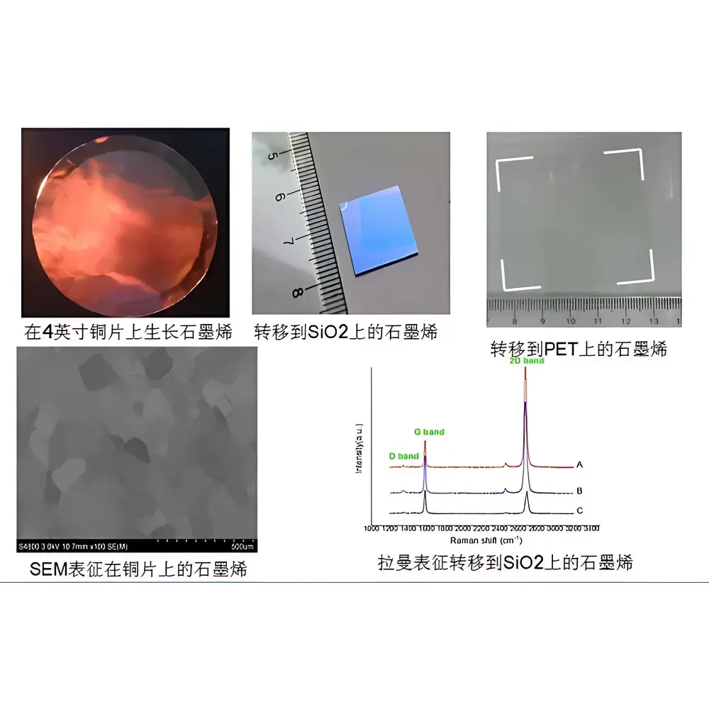
Graphene Materials on Various Substrates are high-quality, transferable graphene films engineered for fundamental research and applied device development in nanoelectronics, optoelectronics, sensor fabrication, and 2D material heterostructure studies. These materials are synthesized via low-pressure chemical vapor deposition (LPCVD) on catalytic metal foils—primarily copper (Cu) and nickel (Ni)—and subsequently transferred onto technologically relevant insulating or transparent substrates using polymer-assisted wet-transfer techniques. The resulting graphene exhibits verified monolayer or few-layer (≤3 layers) continuity, confirmed by Raman spectroscopy (G/2D intensity ratio and full-width-at-half-maximum of the 2D peak), optical contrast analysis, and atomic force microscopy (AFM). Each batch undergoes rigorous quality control in a Class 1000 cleanroom environment, with final packaging performed in ISO Class 5 (100-particle/ft³) clean bags to minimize particulate contamination and preserve surface integrity prior to integration into vacuum or ambient lab processes.
Key Features
- Synthesized on 3.5-inch Cu foil (monolayer dominant) and 4-inch Ni/Cu thin films (tunable layer count via cooling rate and carbon precursor dosage)
- Controlled transfer onto Si/SiO₂ (285 nm oxide), fused silica, quartz, borosilicate glass, and flexible PET substrates — all with dimensions ≤100 mm × 100 mm
- Transfer process optimized to minimize polymer residue, wrinkles, and tear defects; post-transfer annealing available upon request for enhanced carrier mobility
- Batch documentation includes Raman mapping data (≥5 positions per sample), optical micrographs (50×–200×), and sheet resistance values measured by four-point probe (typical range: 300–800 Ω/sq for monolayer on SiO₂)
- Supplied in certified Class 1000 cleanroom environment, packaged in ISO Class 5 clean bags with nitrogen purge and desiccant
Sample Compatibility & Compliance
This graphene product line is compatible with standard semiconductor processing workflows including photolithography, electron-beam lithography, metal evaporation, and atomic layer deposition (ALD). All substrates meet common specifications for surface roughness (Ra 97% at 550 nm for graphene on fused silica). While not certified to ISO 9001 or IATF 16949 as a finished device, manufacturing and handling procedures adhere to GLP-aligned documentation practices—including lot traceability, environmental monitoring logs, and operator gowning protocols—to support reproducibility in academic and industrial R&D settings.
Software & Data Management
No embedded firmware or proprietary software is associated with these graphene materials, as they constitute physical reference standards rather than active instrumentation. However, comprehensive digital documentation is provided with each order: PDF-based Certificate of Analysis (CoA) containing Raman spectra files (.txt/.csv), optical image metadata (EXIF + scale bar), and transfer process parameters (PMMA molecular weight, etchant concentration, rinse duration). Data formats comply with FAIR principles (Findable, Accessible, Interoperable, Reusable) and are structured to integrate with institutional LIMS or ELN platforms such as LabArchives or Benchling. Raw spectral datasets can be exported for third-party analysis using open-source tools (e.g., Python-based RamanTools or WiRE).
Applications
- Calibration and benchmarking of scanning probe microscopy (SPM) and Raman imaging systems
- Gate-tunable field-effect transistor (FET) channel fabrication for transport property characterization
- Transparent conductive electrode evaluation in OLED and perovskite solar cell prototypes
- Surface-enhanced Raman scattering (SERS) substrate development with noble metal nanoparticle decoration
- Model system for interfacial charge transfer studies in hybrid 2D/organic heterojunctions
FAQ
What is the typical monolayer coverage uniformity across a 4-inch transferred film?
Coverage uniformity exceeds 92% over central 75 mm diameter region, verified by large-area Raman mapping (step size ≤10 µm); edge regions may show localized folding or incomplete transfer.
Can you provide graphene on high-resistivity Si (ρ > 10 kΩ·cm) for RF applications?
Yes—custom orders for semi-insulating Si substrates are supported with lead time extension of 10–14 business days.
Is PMMA residue quantified post-transfer, and what cleaning protocols do you recommend?
Residue is assessed qualitatively via XPS C 1s deconvolution and quantitatively via contact angle hysteresis; we recommend acetone/IPA sonication (10 min each) followed by O₂ plasma ashing (50 W, 30 s) for critical applications.
Do you offer electrical characterization data beyond sheet resistance?
Four-point probe mobility extraction (µFE) and Hall effect measurements are available as value-added services upon request, with reporting aligned to ASTM F390-22 guidelines.
Are samples suitable for ultra-high vacuum (UHV) chamber loading without outgassing concerns?
Yes—samples undergo 24-hour vacuum bake-out at 120 °C prior to packaging; total mass loss (TML) < 0.1% per ASTM E595, making them compatible with UHV (<10⁻⁹ Torr) environments.
Related Products
 and Vehicle Classification System")
 System")