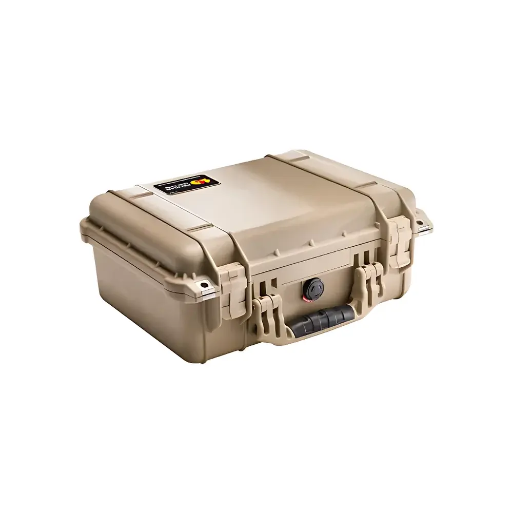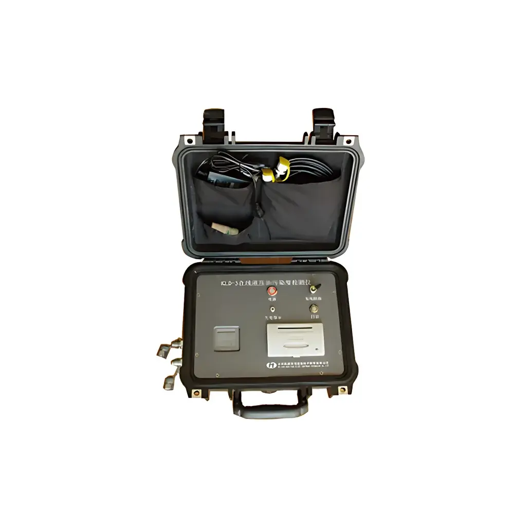
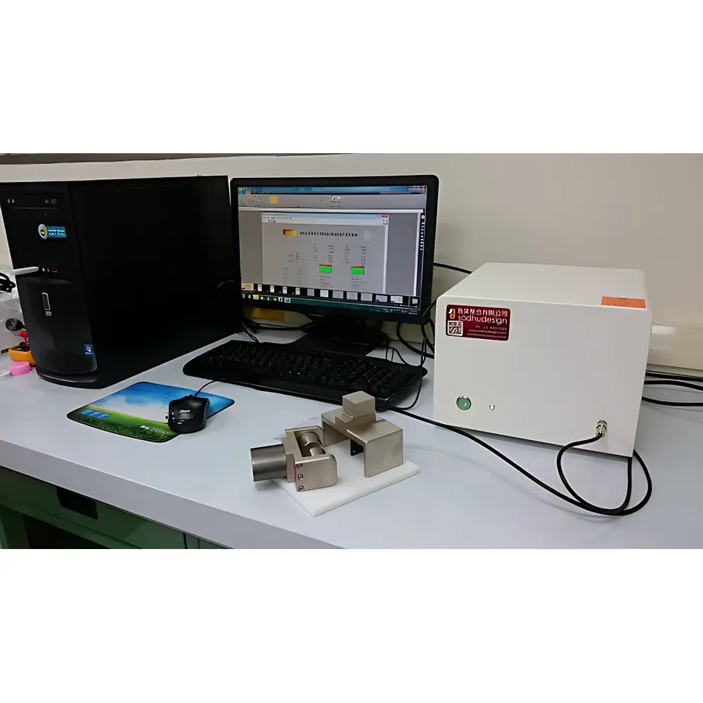
Hall Effect Tester VDP6800 – Variable-Temperature Hall Measurement System with Van der Pauw Configuration
| Key | Origin: Taiwan |
|---|---|
| Manufacturer Type | Authorized Distributor |
| Regional Origin | China (Domestically Assembled) |
| Model | VDP6800 |
| Instrument Type | Variable-Temperature Hall Effect Tester |
| Constant Current Source Range | 1 nA to 20 mA |
| Test Voltage Range | ±10 V |
| Mobility Range | 1–10⁷ cm²/(V·s) |
| Maximum Applied Voltage | 10 V |
| Resistivity Range | 10⁻⁵–10⁷ Ω·cm |
| Carrier Concentration Range | 10⁷–10²¹ cm⁻³ |
| Magnetic Field Options | 0.65 T or 1 T permanent magnet |
| Temperature Capability | Room temperature and liquid nitrogen (77 K) |
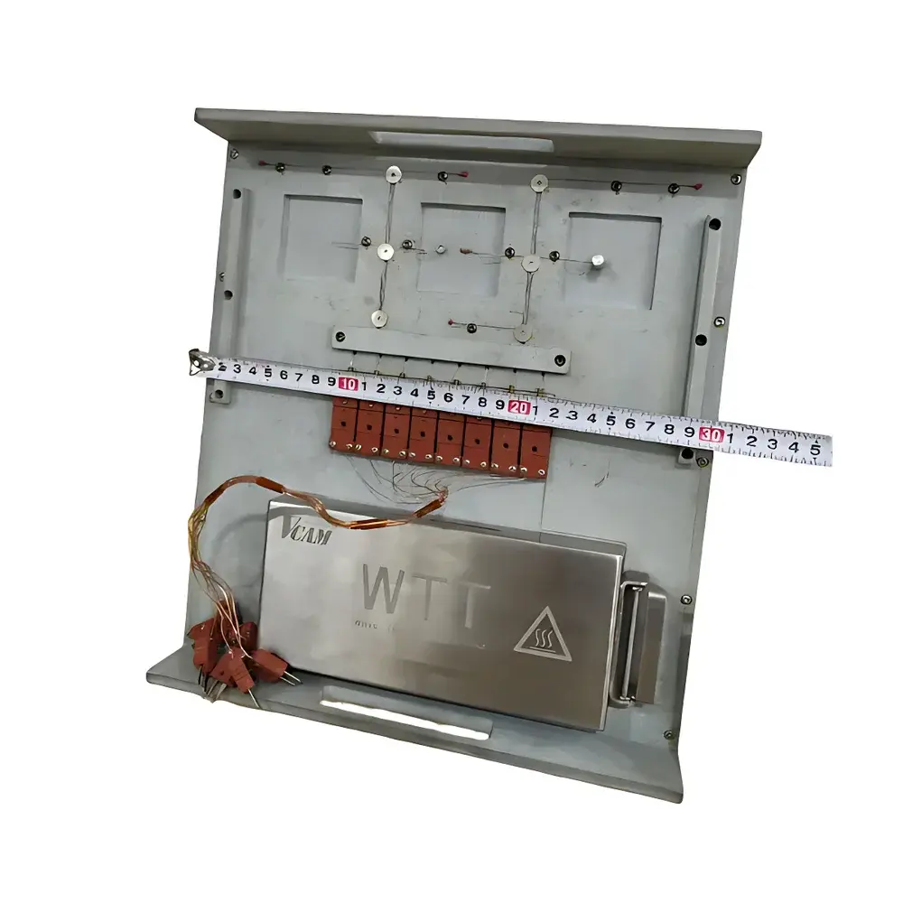
| Sample Holder | Spring-loaded Van der Pauw probe fixture (no sample patterning required) |
| Compatible Materials | Si, ZnO, SiGe, SiC, GaAs, InGaAs, InP, GaN (n-type and p-type) |
| Dimensions (W×D×H) | 260 × 220 × 180 mm |
| Weight | 6 kg |
Overview
The Hall Effect Tester VDP6800 is a benchtop variable-temperature Hall measurement system engineered for precise, reproducible characterization of semiconductor materials using the Van der Pauw (VDP) method. It operates on the fundamental principle of the Hall effect—where a transverse voltage develops across a current-carrying conductor under an applied perpendicular magnetic field—and leverages geometric symmetry to eliminate correction factors associated with sample shape or contact placement. Designed for both bulk and thin-film specimens, the VDP6800 delivers quantitative determination of four critical electronic transport parameters: carrier concentration (bulk and sheet), mobility, resistivity, and Hall coefficient—without requiring lithographically defined Hall bar structures. Its dual-temperature capability (ambient and 77 K) enables thermally activated analysis of carrier freeze-out, scattering mechanisms, and band-edge behavior in wide-bandgap and low-dimensional semiconductors. The system integrates a high-stability permanent magnet (0.65 T or 1 T option), a low-noise programmable current source, and nanovolt-level voltage sensing—all housed in a compact, vibration-insensitive chassis suitable for shared laboratory environments.
Key Features
- Ultra-low-current sourcing: Programmable constant-current output from 1 nA to 20 mA with <0.05% accuracy and sub-picoamp stability—enabling reliable resistivity and Hall measurements on semi-insulating substrates (e.g., semi-insulating GaAs, Al₂O₃-buffered SiC).
- Nanovolt-resolution voltage measurement: Dual-channel 7½-digit electrometer-grade instrumentation capable of ±300 V full-scale range and <10 nV RMS noise floor—critical for accurate Hall voltage extraction under low-field conditions.
- Integrated Van der Pauw spring probe fixture: Patented spring-loaded tungsten carbide probes ensure consistent mechanical pressure and low-contact-resistance (<10 mΩ) across diverse material surfaces—including rough epitaxial layers, transparent conductive oxides, and fragile 2D heterostructures—eliminating the need for photolithography or metal deposition.
- Unified software interface: Single-screen operation workflow guides users through probe configuration, current polarity selection, magnetic field orientation, thermal stabilization confirmation, and automated parameter calculation—reducing operator-induced variability and training overhead.
- I-V linearity verification module: Real-time four-point (A–B–C–D) current–voltage sweep functionality validates ohmic contact quality prior to Hall measurement, flagging non-linearities that would compromise Hall coefficient accuracy per ASTM F76–22 guidelines.
- Modular compatibility: Electrical and mechanical interfaces conform to standard four-point probe (4PP) systems, permitting co-use of shared cryostats, magnet platforms, or vacuum chambers without hardware modification.
Sample Compatibility & Compliance
The VDP6800 supports characterization of all common elemental and compound semiconductors—including Si, Ge, GaAs, InP, GaN, SiC, ZnO, and ternary alloys (e.g., InGaAs, AlGaN)—in both n-type and p-type configurations. Its robust probe design accommodates planar samples ranging from 5 mm × 5 mm to 50 mm × 50 mm, with thicknesses from 100 nm (epitaxial films) to 1 mm (bulk wafers). The system complies with ISO/IEC 17025:2017 requirements for testing laboratories, and measurement traceability aligns with NIST SRM-2135a (Si reference material) protocols. Data acquisition adheres to GLP-compliant audit trails, including timestamped operator ID, environmental logs (temperature, field strength), and raw voltage/current arrays—facilitating FDA 21 CFR Part 11 readiness when integrated with validated LIMS environments.
Software & Data Management
The proprietary HallSoft™ v3.2 application provides real-time visualization of raw sensor data, automatic correction for offset voltages and thermoelectric EMFs, and iterative solving of the Van der Pauw equations under both positive and negative magnetic field polarities. All calculated parameters—including bulk/sheet carrier density, Hall mobility, resistivity, and scattering time—are exported in CSV and XML formats compliant with ASTM E1447–21 data exchange standards. Software includes built-in uncertainty propagation models based on current source tolerance, voltage meter resolution, field homogeneity maps, and contact resistance estimates—generating ISO/IEC Guide 98-3 (GUM)-aligned expanded uncertainties (k=2) for each reported value. Remote operation via TCP/IP is supported for integration into automated wafer-level test platforms.
Applications
- Process development and QC of LED epiwafers: Quantitative assessment of doping uniformity, activation efficiency, and 2DEG formation in AlGaN/GaN HEMT structures.
- Photovoltaic R&D: Correlation of carrier lifetime, defect density, and surface recombination velocity in perovskite and CIGS absorber layers via low-temperature Hall mobility trends.
- Wide-bandgap device qualification: Mobility degradation analysis in SiC MOSFET channels under gate bias stress, linking trap-assisted conduction to Hall-derived carrier freeze-out temperatures.
- Academic materials science: Teaching Van der Pauw methodology, semiconductor physics labs, and graduate research on topological insulators and transition metal dichalcogenides.
- Failure analysis: Identification of interfacial charge trapping at oxide/semiconductor boundaries by comparing room-temperature vs. cryogenic Hall response.
FAQ
Does the VDP6800 require sample patterning or metallization before measurement?
No. The spring-loaded Van der Pauw probe fixture enables direct contact measurement on as-grown or polished surfaces—no lithography, etching, or evaporation steps are needed.
Can the system measure both n-type and p-type semiconductors?
Yes. Automatic polarity reversal of current and magnetic field ensures unambiguous sign determination of the Hall coefficient, distinguishing electron vs. hole conduction with >99.9% confidence.
Is liquid nitrogen handling integrated into the instrument?
The VDP6800 includes a purpose-engineered Dewar mount with thermal isolation gasketing and level-sensing feedback—designed for stable 77 K operation over ≥4 hours without manual refilling.
What calibration standards are recommended for routine verification?
NIST-traceable Si reference wafers (SRM 2135a) and certified GaAs standards (e.g., MTI Corp. HG-100 series) are recommended for quarterly performance checks per ISO/IEC 17025 Clause 7.7.
How does the system handle contact resistance errors in thin-film measurements?
The software applies a modified van der Pauw correction algorithm that incorporates measured contact resistance (from I-V sweeps) into the conductivity tensor inversion—reducing sheet resistance error to <±1.2% for films with Rsheet < 1 kΩ/sq.