Hamamatsu C11011-01W Optical Micrometer Thickness Analyzer
| Brand | Hamamatsu |
|---|---|
| Origin | Japan |
| Manufacturer Type | Original Equipment Manufacturer (OEM) |
| Product Category | Imported Instrument |
| Model | C11011-01W |
| Pricing | Available Upon Request |
| Measurement Principle | Optical Interferometry (Infrared Coherence-Domain Reflectometry) |
| Light Source | Infrared LED (1300 nm) |
| Spot Size | Ø60 µm |
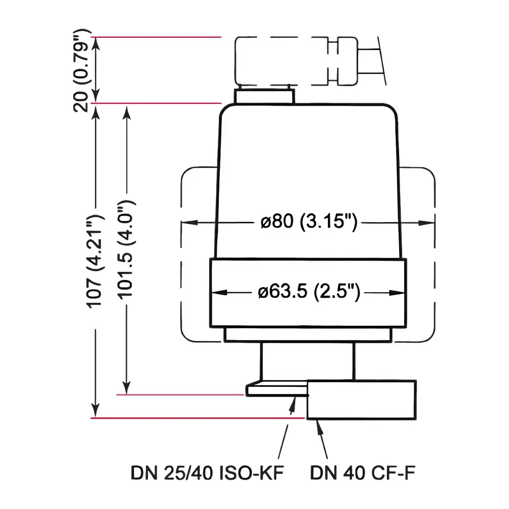
| Working Distance | 155 mm (optional C11011-01WL: 1000 mm) |
| Thickness Range (SiO₂ on Glass) | 25 µm – 2900 µm |
| Thickness Range (Si on SiO₂/Si substrate) | 10 µm – 1200 µm |
| Repeatability (Si film, 6 µm nominal) | ±100 nm (1σ) |
| Accuracy (Si film) | ±0.5 µm for t < 500 µm |
| Measurement Speed | 60 Hz (22.2 ms per point, acquisition only) |
| Layer Capability | Single-layer standard |
| Detection Method | Peak-detection algorithm applied to interference fringe envelope |
| Output Interface | RS-232C, PIPE, USB 2.0 |
| Power Supply | AC 100–240 V, 50/60 Hz |
| Power Consumption | 50 W |
| Compliance | CE-marked |
Overview
The Hamamatsu C11011-01W Optical Micrometer Thickness Analyzer is a non-contact, high-speed interferometric measurement system engineered for in-line and laboratory-based thickness characterization of transparent and semi-transparent thin films on rigid substrates. It operates on the principle of infrared coherence-domain reflectometry—utilizing a stabilized 1300 nm LED source to generate low-coherence interference fringes from optical reflections at film-substrate and air-film interfaces. The system captures the temporal envelope of the interference signal, enabling precise determination of optical path difference and, consequently, physical thickness through calibrated refractive index inputs. Designed for integration into semiconductor fabrication lines, display manufacturing, and precision optics production, the C11011-01W delivers real-time metrology at 60 Hz—sufficient for monitoring moving wafers or continuously conveyed substrates without motion blur or averaging artifacts. Its long working distance (155 mm standard) minimizes mechanical interference with process tooling and accommodates fixtures for warped or patterned samples.
Key Features
- Non-destructive, non-contact measurement using infrared interferometry—enabling thickness quantification of opaque silicon wafers and coated glass without surface contact or vacuum requirements.
- High-speed data acquisition at 60 Hz (22.2 ms per measurement point), optimized for dynamic process monitoring and closed-loop feedback control in automated manufacturing environments.
- Robust optical design with Ø60 µm spot size ensures spatial resolution suitable for mapping localized thickness variations across patterned wafers—including those with microstructures, anti-reflective coatings, or temporary protective films.
- Extended working distance (155 mm) reduces sensitivity to vibration and thermal drift; optional C11011-01WL variant supports up to 1000 mm standoff for integration into confined or shielded process chambers.
- Integrated peak-detection algorithm processes raw interferograms in real time, delivering stable thickness values without requiring user-defined spectral fitting or manual baseline correction.
- Multi-interface connectivity (RS-232C, PIPE, USB 2.0) enables seamless integration with PLCs, SCADA systems, and MES platforms under industry-standard communication protocols.
Sample Compatibility & Compliance
The C11011-01W is validated for single-layer thickness measurement of SiO₂ on glass (25–2900 µm) and silicon-on-insulator or bulk silicon substrates (10–1200 µm). Its 1300 nm illumination penetrates common dielectric passivation layers and polymer protection films, permitting measurement through photoresist, polyimide, or PET overlays without removal. For multi-layer stacks, spectral analysis mode (optional firmware upgrade) supports deconvolution of up to three optically distinct layers when refractive indices are known a priori. The instrument conforms to CE Directive 2014/30/EU (EMC) and 2014/35/EU (LVD); its measurement traceability aligns with ISO/IEC 17025 requirements when used with NIST-traceable reference standards. While not intrinsically compliant with FDA 21 CFR Part 11, audit trails and electronic signature support can be implemented via external software layers meeting GLP/GMP documentation standards.
Software & Data Management
The analyzer operates with Hamamatsu’s proprietary THICKNESS-ANALYZER v3.x suite, providing real-time waveform visualization, statistical process control (SPC) charting, and XY thickness mapping. Raw interferogram data and processed thickness values are exportable in CSV, HDF5, and XML formats—ensuring compatibility with MATLAB, Python (NumPy/Pandas), and JMP for advanced regression modeling. The software supports configurable pass/fail thresholds, alarm triggers, and automated report generation compliant with ISO 9001 documentation workflows. All measurement parameters—including exposure time, gain, and refractive index—are logged with timestamps and operator ID (when integrated with domain authentication). Audit logs record configuration changes, calibration events, and data export actions—meeting foundational requirements for regulated quality systems.
Applications
- Semiconductor front-end process control: monitoring oxide, nitride, and poly-Si film uniformity during CVD, PECVD, and thermal oxidation steps.
- Flat-panel display manufacturing: verifying ITO, SiNx, and organic layer thickness on TFT-LCD and OLED substrates prior to patterning.
- Optical coating QC: validating quarter-wave stack thickness on laser mirrors, filters, and AR-coated lenses.
- MEMS and packaging: measuring polymer encapsulant thickness over bare dies or wafer-level packages.
- R&D labs: characterizing spin-coated photoresists, sol-gel films, and 2D material transfer layers where ellipsometry lacks throughput or step-height profilometry lacks lateral resolution.
FAQ
What substrates and film materials are supported for thickness measurement?
The C11011-01W is optimized for SiO₂, Si₃N₄, Si, and polymer films on silicon, glass, or sapphire substrates. Thickness accuracy assumes known or pre-calibrated refractive indices at 1300 nm.
Can the system measure films on highly reflective or rough surfaces?
Yes—its low-coherence interferometry suppresses speckle noise and tolerates surface roughness up to λ/4 RMS. However, specular reflection loss may require gain adjustment for metals or heavily doped Si.
Is multi-layer analysis included in the base configuration?
Single-layer analysis is standard. Multi-layer capability requires optional firmware license and prior knowledge of layer optical constants.
How is calibration performed and how often is it required?
Factory calibration uses NIST-traceable step-height standards. Field verification is recommended before each production shift using certified reference wafers; full recalibration is advised annually or after optical head servicing.
Does the system support integration with factory automation networks?
Yes—via RS-232C (Modbus RTU), PIPE (Hamamatsu’s deterministic packet protocol), or USB 2.0 HID-class interface, all supporting trigger-in, data-out, and status polling for synchronized operation with conveyors or robotic handlers.