Hamamatsu L9570-01 Stealth Dicing System
| Brand | Hamamatsu |
|---|---|
| Origin | Japan |
| Manufacturer Type | Original Equipment Manufacturer (OEM) |
| Product Origin | Imported |
| Model | L9570-01 |
| Pricing | Available Upon Request |
Overview
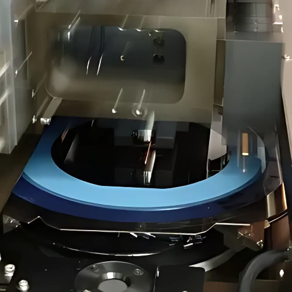
The Hamamatsu L9570-01 Stealth Dicing System is a precision laser-based internal separation platform engineered for high-yield, low-damage dicing of ultra-thin semiconductor wafers. Unlike conventional mechanical dicing—where a rotating diamond blade physically abrades the wafer surface—the L9570-01 employs near-infrared (NIR) ultrafast laser pulses (typically 1030 nm or 1064 nm, depending on optical configuration) focused *within* the bulk material using high-numerical-aperture optics. This nonlinear absorption induces localized micro-modifications—primarily lattice distortion and nanovoid formation—along a predefined cleavage plane, generating a continuous subsurface damage layer (also termed a “stress layer” or “modified region”). Subsequent mechanical stress application (e.g., tape expansion or roller stretching) triggers controlled fracture propagation along this weakened plane, enabling clean, chip-scale separation without surface contact. The system operates under dry, non-contact conditions, eliminating coolant contamination, slurry residue, and mechanical chipping—critical for advanced packaging technologies including fan-out wafer-level packaging (FOWLP), 3D IC stacking, and MEMS device singulation.
Key Features
- Non-contact, dry-process dicing compatible with <100 µm silicon wafers and compound semiconductors (e.g., GaAs, SiC, GaN)
- Subsurface modification via femtosecond or picosecond pulsed NIR laser, minimizing thermal diffusion and collateral damage
- High spatial resolution beam delivery with dynamic focus control for consistent modification depth across warped or patterned wafers
- Integrated wafer alignment subsystem supporting both global (saw street) and local (die-level) registration with sub-micron repeatability
- Real-time process monitoring interface for pulse energy stability, beam position accuracy, and focus drift compensation
- Modular architecture designed for integration into automated semiconductor front-end and back-end production lines (SEMI E10/E15 compliant interfaces)
Sample Compatibility & Compliance
The L9570-01 supports full-wafer processing of silicon (200 mm and 300 mm), SOI, glass, sapphire, and thin-film LED substrates. It accommodates wafer thicknesses from 25 µm to 200 µm, with optimal performance demonstrated at 50–100 µm. All optical and motion components meet ISO 14644-1 Class 5 cleanroom compatibility requirements. The system conforms to IEC 60825-1:2014 (laser safety), SEMI S2-0215 (safety guidelines), and SEMI E10-0215 (defect classification methodology). Process data logging adheres to ALCOA+ principles (Attributable, Legible, Contemporaneous, Original, Accurate, Complete, Consistent, Enduring, Available), supporting GLP/GMP audit readiness and FDA 21 CFR Part 11-compliant electronic records when integrated with validated MES platforms.
Software & Data Management
Control is executed via Hamamatsu’s proprietary DicingMaster™ software suite, providing GUI-driven recipe management, real-time power calibration, multi-point focus mapping, and automatic kerf-width optimization based on material refractive index and thickness input. All process parameters—including pulse energy, repetition rate, scan speed, focal depth, and beam spot size—are logged with timestamp, operator ID, and wafer lot traceability. Export formats include CSV, XML, and HDF5 for statistical process control (SPC) integration. Optional API modules enable bidirectional communication with factory automation systems (FA/SECS-GEM) and yield management databases (YMS).
Applications
- Singulation of ultra-thin logic and memory dies for heterogeneous integration
- Low-k dielectric preservation during dicing of advanced node (≤7 nm) wafers
- Crack-free separation of fragile MEMS sensors and RF front-end modules
- Edge isolation and trench formation prior to TSV (through-silicon via) processing
- Pre-scribing for subsequent plasma dicing or laser lift-off in GaN-on-silicon power devices
- Research-grade internal modification studies in transparent ceramics and photonic crystals
FAQ
What materials are compatible with the L9570-01 besides silicon?
The system supports transparent and semi-transparent substrates including fused silica, sapphire, lithium niobate, and III-V compound semiconductors—provided their bandgap permits nonlinear absorption at the laser wavelength.
Does the L9570-01 require post-processing steps after laser modification?
Yes—mechanical stress application (e.g., tape expansion, roller cleavage, or vacuum chuck release) is required to propagate fracture along the modified layer; no etching or chemical treatment is needed.
Can the system handle patterned wafers with topography?
Yes—autofocus and Z-height tracking compensate for wafer bow and step heights up to ±15 µm within a single scan field.
Is the L9570-01 qualified for high-volume manufacturing environments?
It is designed for 24/7 operation with MTBF > 10,000 hours and supports predictive maintenance via laser diode health monitoring and optical path contamination alerts.
How does stealth dicing impact die strength and reliability testing outcomes?
Studies per JEDEC JEP122G show >20% improvement in die edge strength and reduced infant mortality in accelerated life testing versus blade-diced counterparts, due to absence of microcracks and residual stress concentrations.


