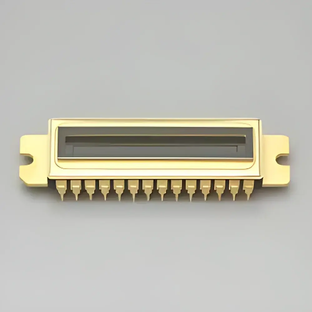
Hamamatsu S11 Series CCD Image Sensors
| Brand | Hamamatsu |
|---|---|
| Origin | Japan |
| Manufacturer Type | Original Equipment Manufacturer (OEM) |
| Import Status | Imported |
| Component Category | Optical Sensor |
| Sensor Architecture | Full-Frame & Interline Transfer CCD |
| Quantum Efficiency | Up to 95% (Back-Illuminated) |
| Fill Factor | 100% (FFT-CCD Technology) |
| Spectral Range | 200–1100 nm |
| Pixel Sizes | 12×12 µm, 14×14 µm, 14×200 µm, 14×500 µm, 14×1000 µm, 24×24 µm, 48×48 µm |
| Array Configurations | Linear (512–4096 px), Area (512×58 to 2048×64 px) |
| Frame Rates | 106–651 fps (area sensors) |
| Specialized Variants | TDI, IR-enhanced, deep-depletion, low-fringing, high-full-well-capacity, integrated electronic shutter |
Overview
The Hamamatsu S11 Series CCD image sensors represent a foundational class of scientific-grade optoelectronic components engineered for high-fidelity photon detection in demanding optical instrumentation. Built upon Hamamatsu’s proprietary Fast-Fourier Transform Charge-Coupled Device (FFT-CCD) architecture, these sensors achieve 100% optical fill factor—eliminating inter-pixel dead space and enabling near-theoretical quantum-limited light collection efficiency. Unlike conventional front-illuminated CCDs, the back-illuminated variants undergo full depletion processing, resulting in extended red/NIR responsivity (up to 1100 nm), reduced etaloning, and enhanced charge transfer efficiency. The S11 platform supports both linear and area array configurations, with pixel geometries optimized for spectral resolution (e.g., elongated 14 × 200 µm pixels for spectroscopic linearity) and spatial fidelity (square 14 × 14 µm or 24 × 24 µm for imaging metrology). These sensors are not standalone cameras but bare-die or ceramic-packaged OEM components intended for integration into spectrometers, ellipsometers, astronomical instrumentation, laser-induced fluorescence systems, and precision photometry platforms where signal integrity, thermal stability, and long-term calibration traceability are critical.
Key Features
- FFT-CCD Architecture: Enables true 100% fill factor and zero geometric light loss—critical for absolute radiometric and photometric applications requiring NIST-traceable calibration.
- Back-Illuminated (BI) Options: Deep-depletion silicon processing delivers >90% peak quantum efficiency (QE) from 400–800 nm and maintains >40% QE beyond 1000 nm—essential for UV-VIS-NIR spectroscopy and low-light Raman detection.
- Low-Fringing Design: Engineered substrate and anti-reflection coating stacks minimize interference fringes in the 600–1100 nm range—improving spectral accuracy in Fourier-transform and grating-based systems.
- OEM-Ready Packaging: Available in hermetically sealed ceramic LCC (Leadless Chip Carrier) and windowed TO-8 packages with optional thermoelectric cooling interfaces for dark current suppression.
- Electronic Shutter Integration: Select linear models (e.g., S11155-2048-01) feature on-chip electronic shuttering—enabling precise exposure control without mechanical components, ideal for pulsed laser synchronization.
- TDI Capability: Time-Delay Integration variants support high-speed scanning applications (e.g., industrial inspection, hyperspectral line-scan imaging) with sub-pixel registration accuracy and motion blur elimination.
Sample Compatibility & Compliance
The S11 series is designed for integration into instruments operating under ISO/IEC 17025-accredited laboratories and regulated environments compliant with FDA 21 CFR Part 11 requirements for electronic records. While the sensor itself is not certified as a final medical or analytical device, its performance characteristics—including stable dark current (99.99% over 95% of full well)—support validation protocols per ASTM E1317 (spectrophotometer performance), ISO 15739 (image sensor noise measurement), and USP (analytical instrument qualification). All devices undergo wafer-level burn-in and parametric testing; Hamamatsu provides full test reports including QE curves, CTE maps, and defect logs—facilitating IQ/OQ documentation for GxP-compliant installations.
Software & Data Management
As bare sensors, S11 devices require external clock drivers, analog signal chain (low-noise correlated double sampling circuitry), and ADC interfacing. Hamamatsu supplies comprehensive hardware reference designs (including timing diagrams, power sequencing schematics, and PCB layout guidelines) and firmware templates compatible with FPGA-based controllers (Xilinx Artix-7, Intel Cyclone V). For system integrators, Hamamatsu’s “CCD Control Software Development Kit” includes LabVIEW VIs, Python APIs (via PyHamamatsu), and C/C++ libraries supporting trigger synchronization, gain/offset calibration, and non-uniformity correction (NUC). Raw frame data output conforms to IEEE 1394b or Camera Link Base configuration—ensuring compatibility with third-party acquisition software such as MATLAB Image Acquisition Toolbox, EPICS IOC drivers, and HALCON SDK. Audit trails, metadata embedding (exposure time, temperature, gain settings), and timestamping are fully implementable at the host controller level to meet GLP/GMP data integrity requirements.
Applications
- High-Resolution Spectroscopy: Linear S11 sensors (e.g., S11151-2048) serve as detectors in benchtop and portable UV-VIS-NIR spectrophotometers, satisfying ASTM E387 linearity and stray light specifications.
- Scientific Imaging: Back-illuminated area arrays (e.g., S11850-1106) enable quantitative fluorescence microscopy, particle tracking velocimetry, and low-light bioluminescence assays with photon-counting capability.
- Astronomical Instrumentation: Low-dark-current, deep-depletion variants operate effectively in cooled focal plane assemblies for ground-based observatories and CubeSat payloads.
- Industrial Metrology: TDI-enabled models perform real-time defect detection on high-speed production lines (e.g., semiconductor wafer inspection, printed circuit board verification).
- Laser Beam Profiling: High dynamic range and sub-pixel centroiding accuracy make S11 sensors suitable for M² measurement systems and wavefront sensing applications.
FAQ
Are S11 sensors supplied with evaluation boards?
No—S11 devices are OEM components only. Evaluation platforms (e.g., C11440 series camera modules) are available separately for prototyping.
What cooling options are supported?
Standard operation supports thermoelectric (Peltier) cooling down to −20°C. Custom vacuum-sealed packages with liquid nitrogen interfaces are available under NDA for ultra-low-noise applications.
Do Hamamatsu provide calibration certificates?
Yes—each wafer lot includes spectral responsivity, QE, and CTE characterization reports. NIST-traceable calibration services are offered via Hamamatsu’s Metrology Center upon request.
Can S11 sensors be used in vacuum or radiation environments?
Certain ceramic-packaged variants meet MIL-STD-883 Class B screening and are qualified for ultra-high vacuum (UHV) use. Radiation-hardened versions require custom qualification.
Is firmware or driver source code provided?
Hamamatsu supplies reference HDL (VHDL/Verilog) for timing generators and open-source C APIs. Proprietary DSP algorithms (e.g., advanced NUC) remain licensed IP.


