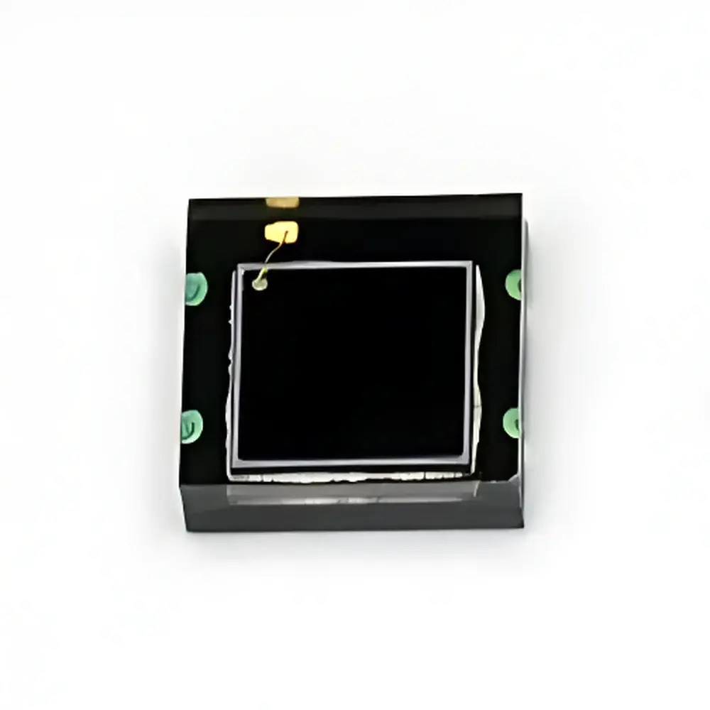
Hamamatsu S12158-01CT Silicon PIN Photodiode
| Brand | Hamamatsu |
|---|---|
| Origin | Japan |
| Manufacturer Type | Original Equipment Manufacturer (OEM) |
| Product Category | Imported Optical Component |
| Model | S12158-01CT |
| Package Type | Chip-on-Board (COB) Surface-Mount |
| Active Area | 2.77 × 2.77 mm |
| Spectral Range | 320–1100 nm |
| Peak Wavelength | 960 nm |
| Responsivity | 0.7 A/W @ 960 nm |
| Dark Current | 10 pA @ VR = 12 V |
| Reverse Voltage (Max) | 20 V |
| Cutoff Frequency | 25 MHz @ VR = 12 V |
| Junction Capacitance | 15 pF @ VR = 12 V |
| Operating Temperature | Ta = 25 °C (typical) |
Overview
The Hamamatsu S12158-01CT is a high-performance silicon PIN photodiode engineered for precision optical detection in visible and near-infrared (VIS-NIR) spectral regimes. Based on a monolithic, planar-doped PIN junction architecture, it delivers stable quantum efficiency across 320–1100 nm with peak responsivity at 960 nm—optimized for applications involving NIR light sources such as 850 nm and 940 nm LEDs, VCSELs, and broadband halogen or tungsten-halogen lamps. Its Chip-on-Board (COB) construction eliminates traditional lead-frame packaging, enabling direct die attachment onto printed circuit boards via reflow soldering. This design supports lead-free assembly processes compliant with JEDEC J-STD-020D moisture sensitivity level (MSL) requirements and RoHS Directive 2011/65/EU. The device operates under reverse bias up to 20 V, ensuring low capacitance (15 pF), high bandwidth (25 MHz cutoff frequency), and minimal dark current (10 pA typical at 12 V), making it suitable for time-resolved photometry, pulsed-light detection, and analog optical signal conditioning in compact instrumentation.
Key Features
- Chip-on-Board (COB) surface-mount package compatible with standard lead-free reflow profiles (peak temperature ≤ 260 °C)
- Compact footprint: 2.77 × 2.77 mm active area with ultra-thin epoxy-glass encapsulation for minimal PCB real estate consumption
- High responsivity of 0.7 A/W at 960 nm—enabling efficient conversion of NIR photons into measurable photocurrent
- Low junction capacitance (15 pF @ VR = 12 V) and fast temporal response (25 MHz bandwidth) for high-speed optical monitoring
- Stable dark current performance (10 pA typical @ VR = 12 V, Ta = 25 °C), supporting low-noise analog front-end design
- Wide spectral coverage from ultraviolet edge (320 nm) through visible to short-wave infrared (1100 nm)
- Designed for industrial-grade reliability under continuous operation in ambient temperatures ranging from –40 °C to +85 °C
Sample Compatibility & Compliance
The S12158-01CT is qualified for integration into systems requiring regulatory alignment with international standards for optoelectronic components. Its lead-free COB structure meets IPC-J-STD-001G requirements for solderability and interconnect integrity. The device complies with IEC 60825-1:2014 for Class 1 laser product safety when used in embedded optical sensing modules. While not certified as a standalone medical device component, its electrical and thermal characteristics support use in IEC 62304-compliant Class B software-driven instruments. Material declarations conform to REACH Annex XIV and conflict minerals reporting per SEC Rule 13p-1. No halogenated flame retardants are employed in the epoxy-glass encapsulant.
Software & Data Management
As a passive analog transducer, the S12158-01CT does not incorporate onboard firmware or digital interfaces. It functions as a current-source element within externally designed signal chains—typically interfaced with transimpedance amplifiers (TIAs), programmable gain instrumentation amplifiers (PGIAs), or analog-to-digital converters (ADCs) in host systems. When integrated into automated test equipment (ATE) or OEM optical analyzers, raw photocurrent output can be digitized and logged under GLP/GMP-aligned data acquisition protocols. Traceability is maintained via calibration certificates referencing NIST-traceable irradiance standards (e.g., FEL-type tungsten lamps calibrated per ISO/IEC 17025). System-level validation may include linearity verification per ASTM E1377–22 and spectral responsivity mapping per ISO 15739:2013.
Applications
- Optical encoders and position sensors in industrial automation and robotics
- NIR reflectance and transmission measurement in portable spectrophotometers and colorimeters
- Pulse oximetry and photoplethysmography (PPG) front-ends in clinical and wearable health monitors
- Laser power monitoring in fiber-coupled diode laser systems (e.g., 808 nm, 915 nm, 976 nm pump sources)
- Flame detection and combustion analysis using dual-wavelength ratio techniques (e.g., 760 nm / 960 nm)
- UV-VIS-NIR reference detectors in laboratory-grade radiometers and integrating sphere setups
- Embedded light-barrier and object-detection modules in smart factory vision systems
FAQ
Is the S12158-01CT compatible with lead-free reflow soldering?
Yes—it is specifically qualified for lead-free reflow processes per JEDEC J-STD-020D, with a maximum peak temperature tolerance of 260 °C.
What is the recommended reverse bias voltage for optimal linearity and speed?
A bias of 12 V is specified for datasheet parameters; operation between 5 V and 15 V maintains >99% linearity across the full photocurrent range.
Can this photodiode be used in vacuum or hermetic environments?
No—the epoxy-glass encapsulation is not rated for vacuum bake-out or long-term hermetic sealing; alternative ceramic-packaged variants (e.g., S12088 series) are recommended for such conditions.
Does Hamamatsu provide spectral responsivity calibration data for individual units?
Standard production units ship with batch-level calibration reports; unit-specific NIST-traceable calibration is available as an optional service (Hamamatsu Part No. CAL-S12158-01CT).
How does temperature affect dark current performance?
Dark current approximately doubles per 10 °C rise above 25 °C; thermal management or correlated double sampling (CDS) techniques are advised for stable operation above 50 °C.


