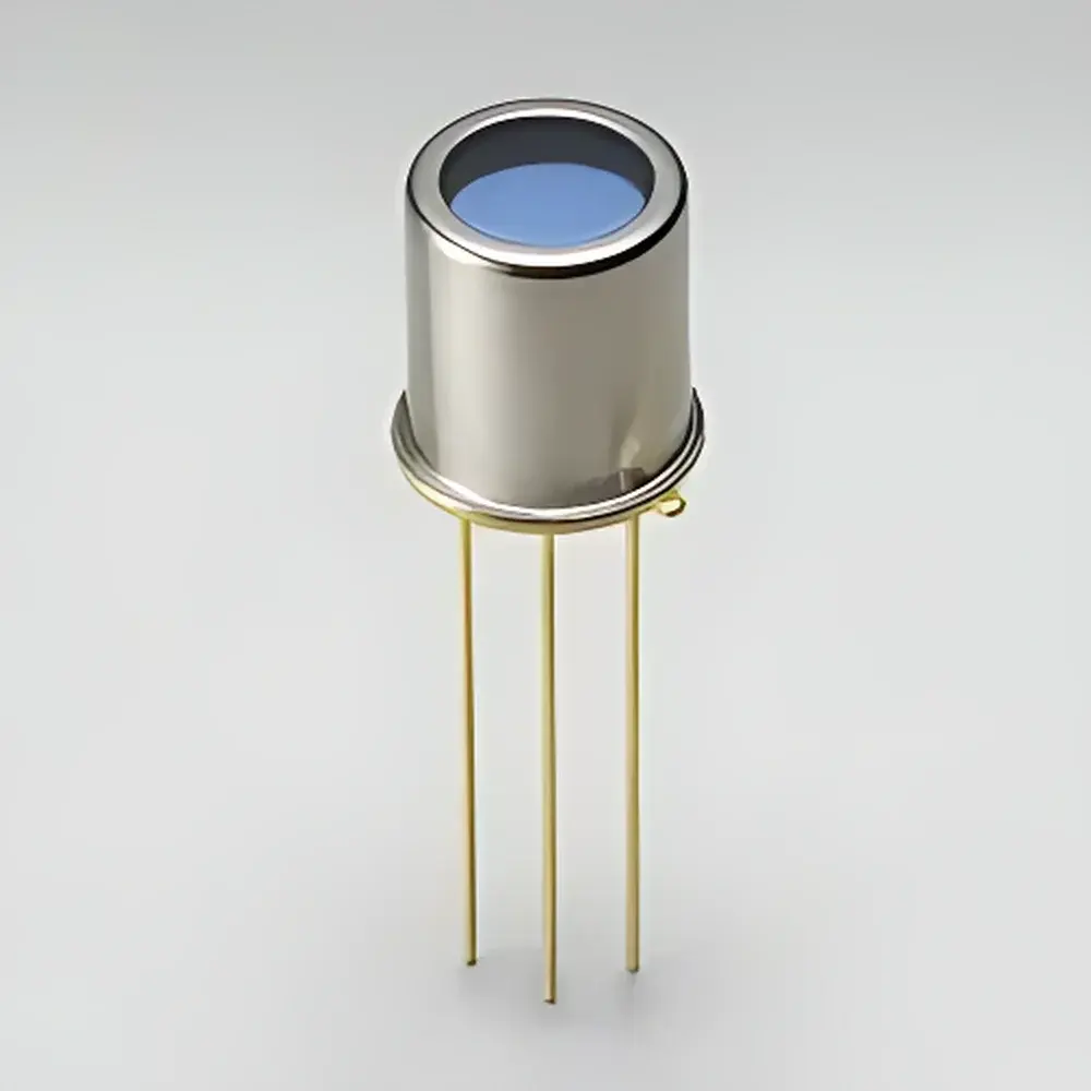
Hamamatsu Silicon Photodiode S12742-220 with Integrated Interference Filter
| Brand | Hamamatsu |
|---|---|
| Origin | Japan |
| Manufacturer Type | Original Equipment Manufacturer (OEM) |
| Product Category | Imported Optical Component |
| Model | S12742-220 |
| Component Type | UV-Specific Photodetector |
| Active Area | 3.6 × 3.6 mm² |
| Spectral Range | 216–224 nm (FWHM ≈ 10 nm) |
| Peak Wavelength (typ.) | 220 nm |
| Responsivity (typ.) | 0.006 A/W @ 220 nm |
| Dark Current (max.) | 25 pA @ VR = 10 mV |
| Reverse Voltage (max.) | 5 V |
| Rise Time (typ.) | 1 µs |
| Junction Capacitance (typ.) | 500 pF @ VR = 0 V, f = 10 kHz |
| Package | Hermetically Sealed Metal Can |
| Cooling | Non-cooled |
| Operating Temperature | Typical at Ta = 25 °C |
Overview
The Hamamatsu S12742-220 is a precision-engineered silicon photodiode optimized for ultraviolet (UV) radiometry in the deep UV spectral region. Unlike broadband photodiodes, this device integrates a hard-coated dielectric interference filter directly onto the entrance window, enabling narrowband spectral selectivity centered at 220 nm with a full width at half maximum (FWHM) of approximately 10 nm. This optical filtering architecture eliminates the need for external monochromators or secondary bandpass filters in applications requiring high spectral purity—such as ozone absorption spectroscopy, UV photolysis monitoring, and calibration of deuterium lamps. The detector operates on the principle of photoelectric conversion in crystalline silicon, where incident photons within the specified 216–224 nm range generate electron-hole pairs proportional to irradiance. Its metal-can hermetic package ensures long-term stability under ambient laboratory conditions and resistance to humidity-induced degradation—a critical requirement for reproducible UV measurements across extended operational cycles.
Key Features
- Integrated interference filter with center wavelength fixed at 220 nm (custom variants available at 340 nm and 560 nm upon OEM request)
- Narrow spectral bandwidth (FWHM ≈ 10 nm) minimizes out-of-band signal contamination and enables high-fidelity monochromatic detection
- 3.6 × 3.6 mm² active area provides sufficient geometric acceptance for collimated beam alignment while maintaining low capacitance
- Non-cooled operation with stable dark current ≤25 pA (measured at VR = 10 mV), suitable for low-noise transimpedance amplifier configurations
- Fast temporal response: typical rise time of 1 µs supports pulsed UV source characterization (e.g., excimer lamp monitoring, laser-induced fluorescence gating)
- Hermetically sealed metal package ensures mechanical robustness, thermal stability, and immunity to environmental oxidation—critical for trace-level UV photometry
- Compliant with JEDEC J-STD-020 moisture sensitivity level (MSL) 1, enabling standard surface-mount handling without baking preconditioning
Sample Compatibility & Compliance
The S12742-220 is designed for integration into optical systems requiring traceable, repeatable UV irradiance measurement. It is compatible with standard UV-grade fused silica optical paths and vacuum-compatible mounting fixtures. As a component-level device—not a finished instrument—it does not carry standalone regulatory certification; however, it meets material and process specifications aligned with ISO 9001-certified manufacturing workflows at Hamamatsu Photonics K.K. (Japan). When incorporated into end-user systems, the diode supports compliance with ASTM E275 (Standard Practice for Describing and Measuring Performance of UV-Vis Detectors) and IEC 62471 (Photobiological Safety of Lamps and Lamp Systems) for hazard classification testing. Its defined spectral responsivity curve facilitates NIST-traceable calibration via primary standard sources such as calibrated deuterium lamps or synchrotron-based transfer standards.
Software & Data Management
As a passive analog sensor, the S12742-220 outputs a photocurrent proportional to incident irradiance and requires external signal conditioning. For data acquisition, it is commonly interfaced with low-noise transimpedance amplifiers (TIAs), lock-in amplifiers (e.g., Zurich Instruments HF2LI), or modular DAQ systems (National Instruments PXIe-4081, Keysight 34972A). Hamamatsu provides comprehensive datasheets—including spectral responsivity curves, temperature-dependent dark current models, and noise-equivalent power (NEP) calculations—for integration into LabVIEW, Python (via PyVISA), or MATLAB-based measurement frameworks. While no proprietary software is bundled, the device’s linear dynamic range (typically >6 decades) and predictable gain drift (<0.05%/°C) simplify implementation of audit-ready measurement protocols compliant with GLP and FDA 21 CFR Part 11 when paired with validated firmware and electronic logging.
Applications
- UV ozone monitoring systems (254 nm absorption reference channels often use 220 nm references for baseline correction)
- In-situ photoreactor dosimetry in semiconductor cleanroom UV curing and water disinfection validation
- Calibration transfer between primary UV radiometric standards and field-deployable spectroradiometers
- Time-resolved detection in UV-pumped fluorescence lifetime systems where spectral isolation prevents Raman/elastic scatter interference
- Beam profiling of excimer lasers (ArF: 193 nm; KrF: 248 nm) using ratio-metric referencing with adjacent filtered detectors
- Development of UV-selective safety interlocks for Class 3B/4 laser enclosures per ANSI Z136.1
FAQ
Can the S12742-220 be used outside its specified 216–224 nm range?
No. The integrated interference filter strongly attenuates radiation beyond ±4 nm from 220 nm. Operation outside this band yields negligible responsivity and risks misinterpretation of stray-light contributions.
Is the device suitable for vacuum ultraviolet (VUV) applications below 200 nm?
No. Silicon transmission cutoff and native oxide absorption limit effective response to wavelengths ≥216 nm. VUV detection requires MgF₂-windowed solar-blind PMTs or CsI photocathodes.
What is the recommended bias configuration?
Zero-bias (photovoltaic mode) is preferred for lowest dark current and highest linearity. Reverse bias up to 5 V may be applied only if faster response is required—but increases dark current exponentially and degrades long-term stability.
How does temperature affect calibration stability?
Responsivity drift is <±0.02%/°C near 220 nm; dark current doubles per ~7 °C rise. For metrologically critical use, thermistor-compensated housing or PID-controlled thermal stabilization is advised.
Does Hamamatsu provide NIST-traceable calibration certificates?
Not for bare components. Traceable calibration must be performed by an accredited lab (e.g., PTB, NPL, or A2LA-accredited providers) after integration into the final optical assembly.


