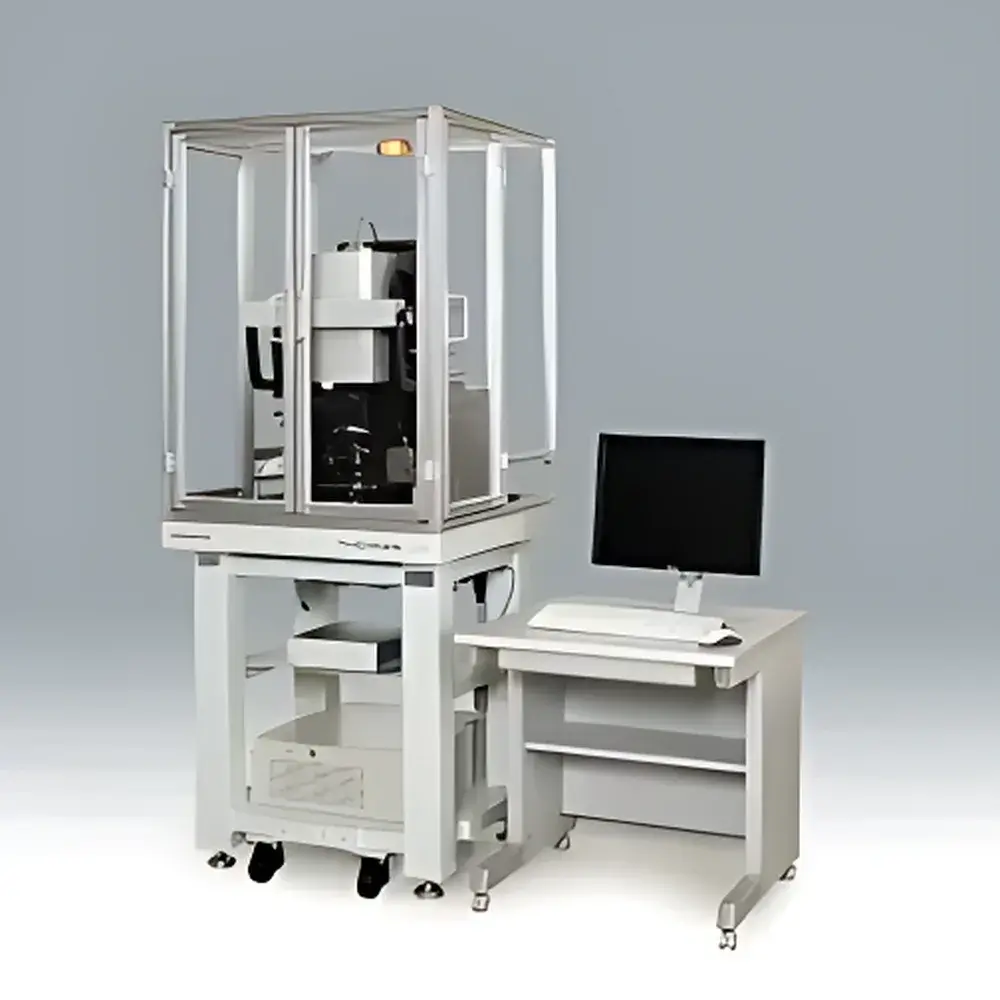
Hamamatsu THEMOS mini Hot-Spot Detection Microscope
| Brand | Hamamatsu |
|---|---|
| Origin | Japan |
| Manufacturer Type | Original Equipment Manufacturer (OEM) |
| Origin Category | Imported Instrument |
| Model | THEMOS mini |
| Pricing | Upon Request |
Overview
The Hamamatsu THEMOS mini is a high-sensitivity, mid-wave infrared (MWIR) hot-spot detection microscope engineered specifically for failure analysis and thermal characterization of semiconductor devices. It operates on the principle of infrared thermography in the 3–5 µm spectral band—where thermal emission from silicon-based microelectronic components is most pronounced under operational bias—and integrates lock-in amplification, Stirling-cycle cooling, and precision optical alignment to resolve sub-millimeter thermal anomalies with exceptional spatial and thermal contrast. Unlike conventional IR cameras or thermographic systems, the THEMOS mini is purpose-built for integration into semiconductor failure analysis (FA) workflows: it enables non-contact, real-time mapping of localized Joule heating, leakage currents, and die-level thermal gradients during electrical stimulation—without requiring device deprocessing or metal layer removal. Its architecture supports both static thermal imaging and dynamic thermal profiling synchronized with external test equipment, making it indispensable for early-stage reliability validation, design-for-test (DFT) feedback loops, and root-cause identification in advanced packaging (e.g., flip-chip, 2.5D/3D ICs) and display technologies (TFT-LCD, OLED).
Key Features
- High-sensitivity InSb focal plane array (640 × 512 pixels, 15 µm pitch) cooled to <80 K via integrated Stirling cryocooler, achieving NETD ≤ 20 mK
- Optimized MWIR optics: standard objective lenses (0.8×, 4×, 15×) and optional ultra-wide-field 0.29× lens (FOV up to 33 × 26 mm) with diffraction-limited performance and zero “water lily” artifacts
- Thermal NanoLens System (optional): immersion-based high-NA optical coupling enabling sub-5 µm effective thermal resolution on uneven surfaces (e.g., bumped wafers, molded packages)
- Lock-in thermography capability (optional): phase-sensitive detection synchronized to AC stimulus, suppressing 1/f noise and enhancing signal-to-noise ratio for low-power leakage localization
- Full hardware synchronization: TTL-triggered acquisition, external clock input, and direct interface with LSI testers via proprietary probe card adapter
- Integrated motorized XYZ stage (8-inch HPK platform), ergonomic eyepiece viewing path, and anti-vibration optical table (standard)
- Real-time video streaming (up to 60 Hz full-frame) with windowing mode for region-of-interest (ROI) acceleration
Sample Compatibility & Compliance
The THEMOS mini accommodates a broad range of semiconductor specimens without modification: bare Si wafers (up to 300 mm / 12-inch), packaged ICs (QFN, BGA, WLCSP), PCB assemblies, TFT-LCD panels, and OLED modules. Sample mounting is facilitated by vacuum chucks and adjustable clamping fixtures compatible with JEDEC-standard carriers. All thermal measurements comply with ASTM E1256-22 (Standard Test Methods for Radiation Thermometers) and ISO 18434-1:2008 (Condition monitoring and diagnostics of machines — Thermography — Part 1: General procedures). When configured with U11389 temperature calibration module, traceable radiometric measurement is achieved per NIST-traceable blackbody references. The system meets electromagnetic compatibility (EMC) requirements per CISPR 11 Class A and safety standards IEC 61010-1 for laboratory use. Data integrity protocols—including audit trails, user access control, and electronic signatures—are implemented in THEMOS Analysis Software to support GLP/GMP and FDA 21 CFR Part 11 compliance in regulated development environments.
Software & Data Management
THEMOS Analysis Software (v5.x, included) provides a unified environment for acquisition, overlay registration, quantitative thermal analysis, and report generation. Core capabilities include: multi-layer image fusion (thermal map + visible template + CAD overlay), pixel-wise ΔT calculation relative to baseline, time-series thermal profiling with timestamped triggers, and automated hotspot centroid extraction with sub-pixel interpolation. Export formats include TIFF (16-bit linear), CSV (temperature matrix), and PDF reports with embedded metadata (instrument ID, operator, test conditions, calibration date). The software supports scripting via Python API for custom analysis pipelines and integrates with industry-standard FA databases (e.g., Synopsys Yield Explorer, PDF Solutions Exensio) via ODBC. All raw thermal frames are stored with embedded EXIF-like headers containing exposure time, gain, cooler status, lens ID, and environmental sensor readings (ambient temperature, humidity, vacuum level).
Applications
- Localization of electromigration-induced metal line shorts and vias opens in advanced logic and memory devices
- Identification of gate oxide breakdown, TDDB-related leakage paths, and micro-plasma events in power MOSFETs and HV ICs
- Thermal mapping of TFT backplanes and organic EL emissive layers to correlate luminance non-uniformity with local heating
- Pre-decap thermal screening of flip-chip packages to guide focused ion beam (FIB) cross-sectioning or laser voltage probing (LVP)
- Dynamic thermal response analysis of 3D-stacked dies under functional test vectors (e.g., memory bandwidth stress, cache coherency traffic)
- Early-design validation: correlating thermal hotspots observed during prototype operation with TCAD simulations to refine layout and power delivery network (PDN) design
FAQ
What is the minimum detectable temperature difference (NETD) of the THEMOS mini?
The system achieves NETD ≤ 20 mK at 30 Hz frame rate with the standard InSb detector and Stirling cooler.
Can the THEMOS mini be used for quantitative temperature measurement?
Yes—when equipped with the U11389 radiometric calibration module and operated within specified ambient and vacuum conditions, it delivers traceable absolute temperature data compliant with ASTM E1256.
Is synchronization with automatic test equipment (ATE) supported?
Yes—via TTL trigger input/output and optional LSI tester interface kit (including probe card adapter and timing controller), enabling stimulus-synchronized thermal capture.
Does the system require liquid nitrogen or external chillers?
No—the integrated Stirling cryocooler eliminates dependency on consumables; only AC power and compressed air (0.5–0.7 MPa) are required for operation.
What is the maximum field of view achievable with the optional 0.29× lens?
Up to 33 mm × 26 mm at working distance 123 mm, enabling macro-scale thermal survey of entire PCBs or large-area displays without stitching.


