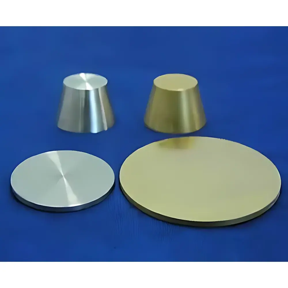
Hefei Kejing Metal Sputtering Targets
| Brand | Hefei Kejing |
|---|---|
| Origin | Anhui, China |
| Manufacturer Type | Authorized Distributor |
| Regional Classification | Domestic (China-made) |
| Model | Metal Sputtering Target |
| Pricing | Available Upon Request |
| Purity Range | 99.9% (3N) to 99.999% (5N) |
| Density | 1.74–21.45 g/cm³ (material-dependent) |
| Standard Diameters | 50.8 mm (2"), 76.2 mm (3"), 60 mm |
| Material Forms | Circular Discs, Custom Shapes Available |
Overview
Hefei Kejing Metal Sputtering Targets are high-performance physical vapor deposition (PVD) materials engineered for precision thin-film fabrication in vacuum environments. Designed for use in magnetron sputtering systems, these targets enable controlled deposition of uniform, stoichiometric metallic films with minimal arcing and high deposition rates. Each target is fabricated via powder metallurgy—including cold isostatic pressing (CIP), high-temperature sintering, and hot isostatic pressing (HIP)—to achieve exceptional density (>99.5% theoretical density), low porosity, and homogeneous microstructure. The metallurgical consistency ensures stable plasma impedance during sputtering, reduced particle generation, and improved film adhesion—critical parameters for optical coatings, semiconductor interconnects, magnetic recording layers, and functionalized architectural glass applications.
Key Features
- High purity grades from 3N (99.9%) to 5N (99.999%), certified per ASTM E1479 and ISO/IEC 17025-accredited analytical methods (ICP-MS, GDMS)
- Density optimized across material families: e.g., Ti (≥4.48 g/cm³), Pt (≥21.35 g/cm³), Al (≥2.69 g/cm³), verified by Archimedes’ principle per ASTM B962
- Dimensional tolerances maintained to ±0.1 mm in diameter and ±0.05 mm in thickness; surface roughness Ra ≤ 0.8 µm (as-sintered) or Ra ≤ 0.2 µm (polished)
- Backplate bonding compatibility: designed for standard indium or epoxy bonding per SEMI F20-0218 specifications
- Trace element control: impurity levels (e.g., Fe, Ni, Cu, O, C) reported on CoA with detection limits <0.1 ppm for key contaminants
Sample Compatibility & Compliance
These targets are compatible with DC, RF, and pulsed DC magnetron sputtering platforms from major OEMs including Applied Materials, ULVAC, Angstrom Engineering, and Denton Vacuum. All materials comply with RoHS Directive 2011/65/EU and REACH Annex XVII restrictions. For regulated industries, traceability is ensured through lot-specific manufacturing records—including raw material batch numbers, sintering profiles, and final dimensional inspection reports. Target packaging adheres to ISO 14644-1 Class 5 cleanroom protocols, with double-bagged VCI (vapor corrosion inhibitor) packaging for long-term storage stability.
Software & Data Management
While sputtering targets themselves are passive components, Hefei Kejing provides full digital documentation support: each shipment includes a Certificate of Analysis (CoA) with elemental composition, density, oxygen content, and grain size distribution (via SEM/EBSD). CoAs are structured in PDF/A-1b format compliant with FDA 21 CFR Part 11 requirements for electronic records. Customers may request integration-ready CSV or XML data exports for LIMS (Laboratory Information Management Systems) or MES (Manufacturing Execution Systems) ingestion. Batch-level metadata—including sintering furnace ID, dwell time, and cooling rate—is retained for ≥10 years per GLP audit standards.
Applications
- Optical Coatings: High-refractive-index Ag and Ti layers for anti-reflective stacks; Au films for plasmonic sensors and IR filters
- Semiconductor Fabrication: Cu and Al targets for interconnect metallization; Ti and Ta for adhesion/barrier layers in advanced node BEOL processes
- Magnetic Storage: CoCrTa and NiFe alloys (custom formulations available) for perpendicular magnetic recording media
- Architectural & Automotive Glass: Low-emissivity (low-E) coatings using Ag–Ni multilayer stacks deposited from segmented targets
- Research & Development: High-purity Mg, Zn, and Cr targets for emerging transparent conductive oxide (TCO) and thermoelectric thin-film studies
FAQ
What purity grade is recommended for semiconductor-grade Cu sputtering?
For sub-45 nm node interconnects, 5N (99.999%) Cu with oxygen content <5 ppm and Fe/Ni/Cr total <1 ppm is strongly advised to prevent electromigration and void formation.
Do you offer bonded targets with Mo or Cu backing plates?
Yes—standard bonding uses high-purity indium (99.99%) or conductive epoxy (e.g., EPO-TEK H20E); custom Mo/Cu backplates are available with thermal expansion matching verification per ASTM E831.
Can I request a target with non-standard geometry (e.g., racetrack or annular shape)?
Custom geometries are supported subject to minimum order quantity (MOQ) and tooling feasibility assessment; lead time extends by 4–6 weeks.
How is grain orientation controlled in Ti targets for improved sputter yield?
Ti targets undergo texture-controlled HIP processing at 1100°C/150 MPa to promote preferred (002) basal plane alignment, enhancing sputter rate reproducibility by ±2.3% over 500 kW·h runtime.
Are CoAs provided with every shipment?
Yes—each lot includes a signed CoA with third-party verification options available upon request (additional fee applies).