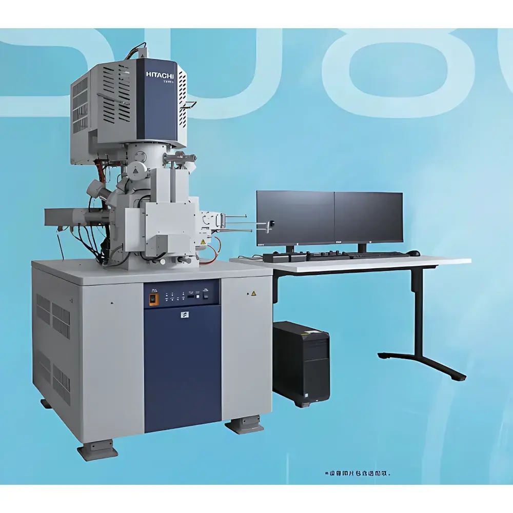
Hitachi SU8600 Series Cold Field-Emission Scanning Electron Microscope
| Brand | Hitachi |
|---|---|
| Origin | Japan |
| Model | SU8600 Series |
| Instrument Type | Floor-Standing SEM |
| Electron Gun | Cold Field Emission |
| Secondary Electron Resolution | 0.6 nm @ 15 kV |
| Magnification Range | 20× to 2,000,000× |
| Accelerating Voltage | 0.5–30 kV |
| Landing Voltage | 0.01–20 kV |
| Maximum Sample Diameter | φ150 mm |
| Detector Options | UD (with ExB energy filter), LD, TD (with energy filter), IMD, PD-BSED, OCD, CLD, STEM Detector |
| Stage | 5-Axis Motorized (X: 0–110 mm, Y: 0–110 mm, Z: 1.5–40 mm, Tilt: −5° to +70°, Rotation: 360°) |
| Software | EM Flow Creator, HD Capture (up to 40,960 × 30,720 px) |
Overview
The Hitachi SU8600 Series is a high-performance cold field-emission scanning electron microscope (CFEG-SEM) engineered for nanoscale imaging, compositional analysis, and structural characterization in advanced materials science, semiconductor R&D, and life sciences laboratories. Leveraging Hitachi’s proprietary cold field emission electron source, the system delivers exceptional brightness, long-term beam stability, and sub-nanometer resolution—critical for low-voltage surface-sensitive imaging and high-current analytical applications. Unlike thermionic or Schottky sources, the cold FEG provides ultra-sharp probe formation with minimal energy spread (<0.3 eV), enabling high-resolution secondary electron (SE) imaging at landing voltages as low as 100 V while maintaining signal-to-noise integrity. The SU8600 integrates a fully electromagnetic lens column with optimized stigmator and alignment systems, supporting both high-magnification topography mapping and quantitative backscattered electron (BSE) contrast analysis across heterogeneous multilayer structures—such as 3D NAND cross-sections, FinFET architectures, and ceramic-metal interfaces.
Key Features
- Cold Field Emission Source with Anode Bake System: Ensures stable, high-brightness electron emission over extended operational periods; includes automated anode conditioning to minimize contamination-induced drift.
- Ultra-High Resolution Imaging: 0.6 nm SE resolution at 15 kV and 0.7 nm at 1 kV, validated per ISO 16700:2016 standards for SEM resolution measurement.
- Advanced BSE Detection Architecture: Incorporates multiple detector configurations—including the novel Oxide-based Cathodoluminescence Detector (OCD)—enabling sub-second acquisition of high-contrast, depth-resolved BSE images without compromising spatial fidelity.
- Multi-Channel Simultaneous Acquisition: Native support for up to six independent signals (SE, BSE, CL, STEM, EDS, EBSD) displayed and saved concurrently, facilitating correlative microscopy workflows.
- Motorized 5-Axis Precision Stage: Enables reproducible positioning within ±0.1 µm accuracy; tilt range from −5° to +70° supports cross-sectional analysis and crystallographic orientation mapping.
- Dual-Monitor Native UI: Optimized for ergonomic operation; primary display dedicated to real-time imaging and navigation, secondary screen reserved for parameter control, scripting interface, and metadata logging.
Sample Compatibility & Compliance
The SU8600 accommodates specimens up to 150 mm in diameter and 50 mm in height, compatible with standard SEM stubs, wafer carriers, and custom holders for in situ heating/cooling stages (optional). Its vacuum architecture maintains base pressure <2 × 10⁻⁸ Pa in the gun chamber and <5 × 10⁻⁴ Pa in the sample chamber—meeting ASTM E1508-21 requirements for analytical SEM environments. All detectors and stage controllers comply with IEC 61000-6-2/6-3 for electromagnetic compatibility. For regulated environments, optional software modules support 21 CFR Part 11-compliant audit trails, electronic signatures, and secure user role management—fully aligned with GLP and GMP documentation protocols.
Software & Data Management
EM Flow Creator serves as the core automation platform, offering drag-and-drop workflow construction for repeatable image acquisition sequences—e.g., multi-site survey → focus optimization → high-resolution capture → EDS point analysis → report export. Each module (magnification setting, stage movement, contrast/brightness adjustment, dwell time selection) is scriptable and timestamped. HD Capture enables lossless tiling of ultra-large format images (up to 40,960 × 30,720 pixels), stored in TIFF or HDF5 format with embedded metadata (accelerating voltage, working distance, detector gain, stage coordinates). Raw data exports are compatible with third-party quantification tools including DigitalMicrograph, ImageJ/Fiji, and Thermo Scientific Avizo.
Applications
- Semiconductor failure analysis: Cross-sectional imaging of gate-all-around transistors, trench isolation layers, and Cu/low-k interconnect stacks.
- Advanced battery materials: Nanoscale mapping of SEI layer morphology on Si-anodes and cathode particle cracking after cycling.
- Geological thin sections: Phase discrimination via atomic number contrast using filtered BSE signals from TD and IMD detectors.
- Biological ultrastructure: Low-kV imaging of non-conductive, unstained tissue sections with charge compensation via beam deceleration mode.
- Metallurgical grain boundary analysis: Integrated EBSD pattern indexing synchronized with topographic SE imaging for crystallographic texture correlation.
FAQ
What vacuum level does the SU8600 maintain in the electron gun chamber?
The cold field emission gun operates under ultra-high vacuum conditions, with a base pressure better than 2 × 10⁻⁸ Pa maintained by a combination of ion pumps and NEG (non-evaporable getter) elements.
Is the OCD detector compatible with elemental mapping?
No—the OCD is optimized for fast, high-contrast BSE imaging; elemental mapping requires integration with an energy-dispersive X-ray spectrometer (EDS) or wavelength-dispersive spectrometer (WDS).
Can EM Flow Creator routines be exported for use on other Hitachi SEMs?
Yes—workflows are saved in XML-based format and are interoperable across the Regulus and SU series platforms running firmware v4.2 or later.
Does the SU8600 support beam deceleration mode?
Yes—landing voltage is independently adjustable from accelerating voltage (0.01–20 kV), enabling surface-sensitive imaging with minimized charging and subsurface excitation.
What is the maximum frame size supported by HD Capture during tiled acquisition?
HD Capture supports stitched mosaics up to 40,960 × 30,720 pixels, with automatic overlap correction and geometric distortion compensation applied in real time.


