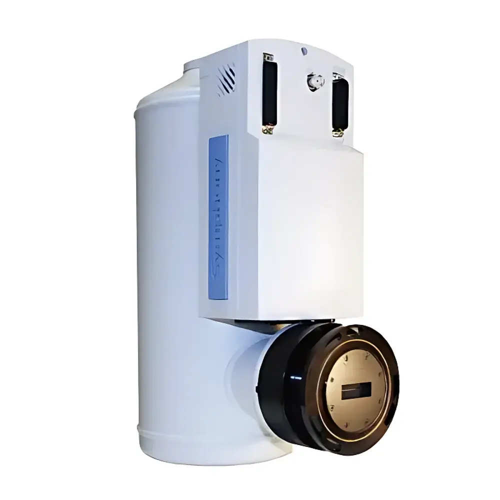
HORIBA IGA Array InGaAs Linear Detector
| Brand | HORIBA |
|---|---|
| Origin | USA |
| Manufacturer Type | Manufacturer |
| Import Status | Imported |
| Model | IGA Array |
| Pricing | Available Upon Request |
| Spectral Range | 0.8–1.7 µm and 1.0–2.2 µm |
| Cooling Options | Thermoelectric (TE) or Liquid Nitrogen (LN₂) |
| Pixel Configurations | 512×1, 1024×1 |
| Pixel Sizes | 25 µm × 250 µm, 25 µm × 500 µm, 50 µm × 250 µm, 50 µm × 500 µm |
| Operating Temperature (LN₂) | –103 °C |
| Software Integration | SynerJY®, SDK, LabVIEW® VIs |
Overview
The HORIBA IGA Array is a high-performance linear InGaAs (Indium Gallium Arsenide) photodetector engineered for demanding near-infrared (NIR) spectroscopic applications requiring exceptional sensitivity, low-noise operation, and spectral fidelity across two critical NIR windows: 0.8–1.7 µm and 1.0–2.2 µm. Unlike silicon-based detectors limited to visible and short-wave NIR, the IGA Array leverages the intrinsic quantum efficiency of InGaAs to deliver robust photon detection in regions where molecular overtone and combination bands dominate—enabling precise analysis of C–H, O–H, and N–H vibrations in pharmaceuticals, polymers, agricultural samples, and semiconductor materials. Its monolithic linear array architecture—available in 512- and 1024-pixel configurations—ensures high spatial resolution along the dispersion axis when coupled with HORIBA Jobin Yvon spectrometers, supporting both scanning and full-spectrum acquisition modes. The detector operates on fundamental photovoltaic principles, generating charge carriers proportional to incident photon flux, with signal integrity preserved through optimized readout electronics and deep cooling.
Key Features
- Cryogenic Noise Suppression: Dual cooling pathways—thermoelectric (TE) and liquid nitrogen (LN₂)—enable stable operation down to –103 °C. LN₂ cooling reduces dark current by up to three orders of magnitude versus uncooled operation, essential for long integration times and ultra-low-light measurements such as Raman spectroscopy or diffuse reflectance of biological tissues.
- Dynamic Range Optimization: Two selectable acquisition modes—High Sensitivity Mode and High Dynamic Range Mode—are implemented via firmware-controlled gain and integration time adjustments. This allows users to prioritize signal-to-noise ratio (SNR) in weak-signal regimes or preserve linearity over four decades of intensity variation without saturation.
- Precision Pixel Architecture: Multiple pixel geometries—including 25 µm × 250 µm, 25 µm × 500 µm, 50 µm × 250 µm, and 50 µm × 500 µm—are offered to balance spectral resolution, étendue matching, and responsivity. Narrower pixels enhance resolving power in high-resolution grating systems; taller pixels increase fill factor and quantum efficiency for low-throughput optical paths.
- Linearity & Stability: Demonstrated >99.9% linearity across full well capacity ensures quantitative accuracy required for ASTM E1421-compliant NIR method validation and USP spectroscopic assay protocols. Gain drift remains below ±0.05% per hour under thermal equilibrium conditions.
Sample Compatibility & Compliance
The IGA Array is designed for integration into Class I laser-safe optical benches and ISO/IEC 17025-accredited laboratory environments. Its sealed, vacuum-compatible housing prevents moisture ingress during LN₂ operation and meets MIL-STD-810G environmental robustness requirements. When deployed with HORIBA’s modular spectrometer platforms (e.g., iHR series), the system supports compliance with FDA 21 CFR Part 11 through SynerJY®’s audit-trail-enabled acquisition logs, electronic signatures, and secure user-role management. All configurations adhere to RoHS Directive 2011/65/EU and CE marking requirements for electromagnetic compatibility (EN 61326-1) and safety (EN 61010-1).
Software & Data Management
Native control and data acquisition are executed via SynerJY®, HORIBA’s unified spectroscopy software platform compliant with GLP/GMP workflows. SynerJY® provides real-time spectral preview, multi-channel co-adding, cosmic-ray rejection, and non-uniformity correction (NUC) using factory-measured pixel response maps. For custom automation, the IGA Array exposes a comprehensive Windows-compatible Software Development Kit (SDK) supporting C/C++, .NET, and Python interfaces. LabVIEW® VIs—certified for NI LabVIEW 2019–2023—are provided for seamless integration into automated QC lines, process analytical technology (PAT) frameworks, and academic research rigs requiring hardware-level timing synchronization (e.g., gated detection synchronized to pulsed lasers).
Applications
- Pharmaceutical solid-state characterization (polymorph identification, hydrate quantification)
- In-line monitoring of polymer extrusion and film casting processes
- Non-destructive quality control of lithium-ion battery electrode coatings
- Soil organic carbon and moisture content mapping via field-portable NIR systems
- Gas-phase absorption spectroscopy of hydrocarbons and greenhouse gases (CH₄, CO, N₂O)
- Time-resolved photoluminescence decay studies in III-V semiconductor heterostructures
FAQ
What spectral calibration standards are recommended for IGA Array systems?
NIST-traceable tungsten-halogen and rare-earth oxide (e.g., Holmium Oxide) filters are advised for wavelength calibration; certified blackbody sources (e.g., PRM-1000) are used for radiometric validation.
Can the IGA Array be operated in vacuum or inert-gas purged enclosures?
Yes—the detector head features a CF-35 flange option and is rated for operation under ≤10⁻³ mbar vacuum or nitrogen-purged atmospheres to minimize atmospheric water vapor absorption in the 1.8–2.0 µm region.
Is firmware update capability available remotely?
Firmware updates are delivered via SynerJY®’s integrated updater module and require physical USB connection for security-critical bootloader verification.
How does pixel binning affect effective resolution and SNR?
Hardware binning (2×1, 4×1) is supported in SDK mode, trading spectral resolution for ~√N improvement in SNR and reduced readout noise—ideal for rapid screening applications where absolute resolution is secondary to throughput.
What is the typical dark current specification at –80 °C under TE cooling?
Measured median dark current is 50–120 e⁻/pixel/s at –80 °C for 25 µm × 500 µm pixels, depending on bias voltage and integration time—values are documented in individual unit test reports shipped with each detector.


