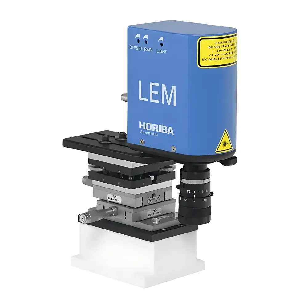
HORIBA LEM IEP Laser Interferometric Endpoint Detector
| Brand | HORIBA |
|---|---|
| Origin | France |
| Manufacturer Type | Original Equipment Manufacturer (OEM) |
| Import Status | Imported |
| Model | LEM |
| Pricing | Available Upon Request |
Overview
The HORIBA LEM IEP is a precision laser interferometric endpoint detector engineered for real-time, non-contact monitoring of thin-film thickness and trench depth during plasma-based dry etching and physical/chemical vapor deposition (PVD/CVD) processes. Operating on the principle of optical interference in a Michelson or modified Fabry–Pérot configuration, the system directs a collimated monochromatic laser beam onto the wafer surface at near-normal incidence. Reflected light from both the top interface (e.g., air/film) and underlying interfaces (e.g., film/substrate) recombines coherently, generating an interference signal whose intensity oscillates as a function of optical path difference. Each full interference fringe corresponds to a physical displacement of λ/2n, where λ is the selected laser wavelength and n is the refractive index of the etched or deposited layer. This deterministic relationship enables quantitative, sub-nanometer resolution tracking of process dynamics—critical for high-yield semiconductor manufacturing, MEMS fabrication, and compound semiconductor device processing.
Key Features
- Three selectable laser wavelengths: 670 nm (visible), 905 nm, and 980 nm (NIR), optimized for broad material compatibility—including SiO₂, Si₃N₄, GaAs, InP, AlGaAs, GaN, and metal stacks.
- Integrated digital CCD imaging subsystem providing real-time top-down visual feedback; enables precise alignment and verification of laser spot position on patterned wafers without breaking vacuum.
- Modular mechanical design allowing direct integration into standard RIE, ICP, PECVD, and sputtering chambers with minimal footprint and no modification to existing chamber geometry.
- High-stability interferometric optics with temperature-compensated mounting and vibration-damped housing—engineered for continuous operation in high-RF, high-vacuum industrial environments.
- Real-time fringe acquisition at up to 10 kHz sampling rate, supporting both simple fringe counting and advanced spectral envelope analysis for multi-layer or gradient-index film characterization.
Sample Compatibility & Compliance
The LEM IEP supports 100 mm to 300 mm diameter wafers, including bare silicon, SOI, sapphire, quartz, and compound semiconductor substrates. Its wavelength flexibility ensures optimal signal-to-noise ratio across dielectric, semiconductor, and metallic films—particularly where absorption or transparency limits conventional reflectometry. The system complies with SEMI S2/S8 safety standards for semiconductor equipment and meets electromagnetic compatibility (EMC) requirements per EN 61326-1 for industrial measurement devices. All optical components are certified for Class 1 laser safety (IEC 60825-1:2014) when installed per HORIBA’s integration guidelines. Data integrity protocols align with GLP and GMP expectations, supporting audit-ready timestamping and metadata logging.
Software & Data Management
The LEM IEP is operated via HORIBA’s proprietary endpoint monitoring software, pre-installed on a Windows 10 Pro 64-bit industrial PC. The software provides synchronized visualization of raw interference signals, normalized fringe envelopes, derivative-based rate estimation, and user-defined endpoint thresholds. It supports scripting (via Python API) for automated recipe-driven control, integration with SECS/GEM host interfaces, and export of time-stamped datasets in HDF5 and CSV formats. Audit trail functionality records all parameter changes, operator logins, and measurement events in accordance with FDA 21 CFR Part 11 requirements for electronic records and signatures. Calibration history, instrument configuration snapshots, and spectral reference libraries are stored in encrypted local databases with optional network backup.
Applications
- Endpoint detection in gate oxide etch, STI recess, and hard mask removal for logic and memory fabs.
- In-situ monitoring of ALD and PEALD cycles for ultra-thin film uniformity validation.
- Depth profiling of deep silicon etches (Bosch process) and TSV formation with sub-5 nm repeatability.
- Real-time control of III–V epitaxial layer growth termination in MOCVD reactors.
- Characterization of interfacial oxidation or nitridation kinetics during thermal treatments.
FAQ
What laser wavelength should I select for SiO₂ on Si?
For thermal SiO₂ on silicon, 905 nm offers optimal penetration depth and fringe contrast; 670 nm may be preferred for very thin (<10 nm) layers where visible-light sensitivity improves signal fidelity.
Can the LEM IEP distinguish between multiple stacked layers?
Yes—by combining multi-wavelength measurements and modeling interference spectra using transfer-matrix methods, the system supports qualitative layer differentiation and semi-quantitative thickness estimation in bilayer and trilayer structures.
Is vacuum feedthrough included with the system?
Standard configurations include a CF-63 or ISO-KF 50 vacuum-compatible optical feedthrough with anti-reflective coated fused silica window; custom flange types (e.g., DN100, ConFlat) are available upon request.
Does the software support remote monitoring via Ethernet?
Yes—the software includes a secure HTTP(S) server mode enabling browser-based access to live signals, historical trends, and alarm status from any networked workstation within the fab intranet.
How is calibration performed and how often is it required?
Factory calibration is traceable to NIST standards and includes wavelength accuracy, optical path stability, and pixel-to-position mapping; field recalibration is not routine but recommended annually or after major mechanical intervention.
Related Products
")