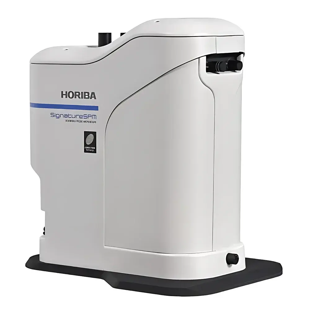
HORIBA Signature SPM Chemical Atomic Force Microscope
| Brand | HORIBA |
|---|---|
| Origin | France |
| Manufacturer Type | Manufacturer |
| Import Status | Imported |
| Model | Signature SPM |
| Instrument Category | Atomic Force Microscope |
| Instrument Type | Materials-Focused AFM |
| Spectroscopy Integration | Confocal Raman & Photoluminescence (PL) |
| Core Capability | True Co-Localized Multimodal Imaging (Topography + Nanomechanics + Electrostatics + Magnetism + Chemical Fingerprinting) |
| Scanner Range | 100 × 100 × 15 µm |
| Optical Access | Dual-Path, IR AFM Laser (1310 nm) + Visible/NIR Excitation Lasers (e.g., 532 nm, 638 nm, 785 nm) |
| Spectrometer | Achromatic, >95% Reflectivity, Triple-Grating Support (150–6000 cm⁻¹) |
| Software Feature | “Probe Away” / “Probe Back” Automated Tip Retraction & Re-Registration |
| Compliance | Designed for GLP/GMP-adjacent research environments |
Overview
The HORIBA Signature SPM is a purpose-engineered chemical atomic force microscope that unifies high-resolution nanoscale physical characterization with molecular-level chemical identification in a single, spatially registered measurement platform. Unlike conventional correlative approaches requiring sequential or offline alignment, the Signature SPM implements true co-localized multimodal imaging—simultaneously acquiring topographic, mechanical, electrical, magnetic, and spectroscopic data from the exact same nanoscale region. Its core architecture separates the AFM optical path (using a 1310 nm infrared laser diode) from the visible/NIR excitation path for Raman and photoluminescence (PL), eliminating spectral crosstalk and enabling quantitative, artifact-free chemical mapping on light-sensitive samples—including biological membranes, organic semiconductors, perovskite photovoltaics, and quantum dot arrays. The system operates on the principle of probe-based force detection (contact, tapping, and non-contact modes) coupled with confocal micro-Raman spectroscopy and time-resolved PL, delivering metrologically traceable nanomechanical properties alongside vibrational and electronic band structure information.
Key Features
- True co-localization without registration drift: Proprietary “Probe Away” software command retracts the cantilever fully from the sample surface while preserving stage coordinates, enabling unobstructed confocal Raman/PL mapping; “Probe Back” returns the tip to the prior analysis position within ≤3 µm repeatability—no manual realignment required.
- Dual-path optical architecture: Independent optical pathways for AFM detection and spectroscopic excitation ensure zero interference between the 1310 nm AFM laser and visible/NIR Raman/PL lasers (e.g., 532 nm, 638 nm, 785 nm), critical for photolabile and carrier-sensitive materials.
- Full-spectrum spectroscopy integration: High-throughput achromatic spectrometer with >95% average reflectivity and triple-grating support enables seamless switching across spectral ranges (150–6000 cm⁻¹), optimized for both low-frequency lattice modes and high-energy electronic transitions.
- Metrological AFM performance: 100 × 100 × 15 µm closed-loop scanner delivers sub-nanometer height resolution, low thermal drift (<0.5 nm/min), and fast response dynamics—validated against NIST-traceable standards per ASTM E2534.
- Comprehensive AFM modality suite: All major scanning probe techniques are included as standard: Kelvin Probe Force Microscopy (KPFM), Piezoresponse Force Microscopy (PFM), Magnetic Force Microscopy (MFM), nanolithography, and quantitative force-curve spectroscopy.
- Automated alignment subsystem: Fully motorized laser, cantilever, and photodiode alignment eliminates user-dependent setup variability and ensures consistent signal-to-noise ratios across operators and sessions.
Sample Compatibility & Compliance
The Signature SPM accommodates a broad range of solid-state and soft matter specimens—from conductive 2D materials (graphene, MoS₂) and oxide thin films to hydrated biological sections, polymer blends, and semiconductor heterostructures. Its non-invasive optical design and IR-based AFM detection preserve sample integrity during extended acquisition. The system supports vacuum, ambient, and liquid-cell configurations (optional). From a regulatory standpoint, the hardware architecture and optional software modules comply with foundational requirements for data integrity in regulated research: full audit trail logging, electronic signature support, and exportable metadata compliant with FAIR principles. While not a GMP-certified instrument per se, its metrological traceability, calibration documentation, and repeatable tip exchange protocol align with ISO/IEC 17025 laboratory accreditation frameworks and facilitate FDA 21 CFR Part 11–compliant workflows when deployed with validated software configurations.
Software & Data Management
HORIBA’s LabSpec 8 platform serves as the unified control and analysis environment for the Signature SPM. It provides synchronized acquisition triggers, real-time overlay of AFM topography with Raman/PL intensity maps, and pixel-by-pixel spectral fitting (e.g., Lorentzian/Gaussian deconvolution, bandgap extraction, strain quantification). All raw data—including force curves, spectroscopic stacks, and positional metadata—are stored in vendor-neutral HDF5 format with embedded calibration parameters. Batch processing pipelines support automated baseline correction, cosmic ray removal, and multivariate statistical analysis (PCA, cluster mapping). For laboratories requiring compliance documentation, optional software packages deliver electronic logbooks, user access controls, and version-controlled method templates—all designed to support GLP audits and reproducible cross-laboratory studies.
Applications
- Materials Science: Correlating local strain fields (via Raman peak shifts) with nanomechanical modulus gradients (via force-volume mapping) in piezoelectric oxides and flexible electronics.
- Semiconductor R&D: Identifying defect-related PL quenching zones adjacent to dislocation networks imaged via phase contrast AFM—critical for GaN HEMT and SiC power device development.
- Nanophotonics: Mapping plasmonic hotspots (via tip-enhanced Raman scattering readiness) alongside surface potential variations (KPFM) on Au nanoantennas.
- Energy Materials: Quantifying ion migration pathways in solid-state electrolytes by combining electrochemical strain microscopy (ESM) with localized Li–O vibrational signatures.
- Life Sciences: Imaging amyloid fibril morphology (tapping-mode AFM) while simultaneously detecting β-sheet conformational markers (1670 cm⁻¹ amide I band) in native tissue sections.
FAQ
Does the Signature SPM require external vibration isolation?
Yes. As with all high-resolution SPM systems, optimal performance necessitates active or passive vibration isolation appropriate for the lab environment—especially for sub-Å topographic stability and low-noise force spectroscopy.
Can the system perform time-resolved PL measurements?
Yes. When configured with a pulsed laser source and time-correlated single-photon counting (TCSPC) module (optional), the Signature SPM supports nanosecond-resolved PL lifetime mapping co-registered with AFM topography.
Is tip exchange fully automated?
Tip exchange is operator-independent and highly reproducible, but physical cantilever mounting remains manual. The system automatically re-registers the new tip’s optical alignment and repositions it to the prior scan location using calibrated stage coordinates.
What Raman laser wavelengths are supported out-of-the-box?
Standard configurations include 532 nm, 638 nm, and 785 nm lasers; custom wavelengths (e.g., 405 nm, 830 nm) can be integrated upon request, subject to optical path compatibility verification.
How is calibration traceability maintained across modalities?
Scanner linearity is verified using NIST-traceable step-height standards; Raman wavenumber accuracy is calibrated using neon or silicon reference spectra; force sensitivity is validated via thermal tune and Sader methods—all documented in the system’s calibration report archive.


