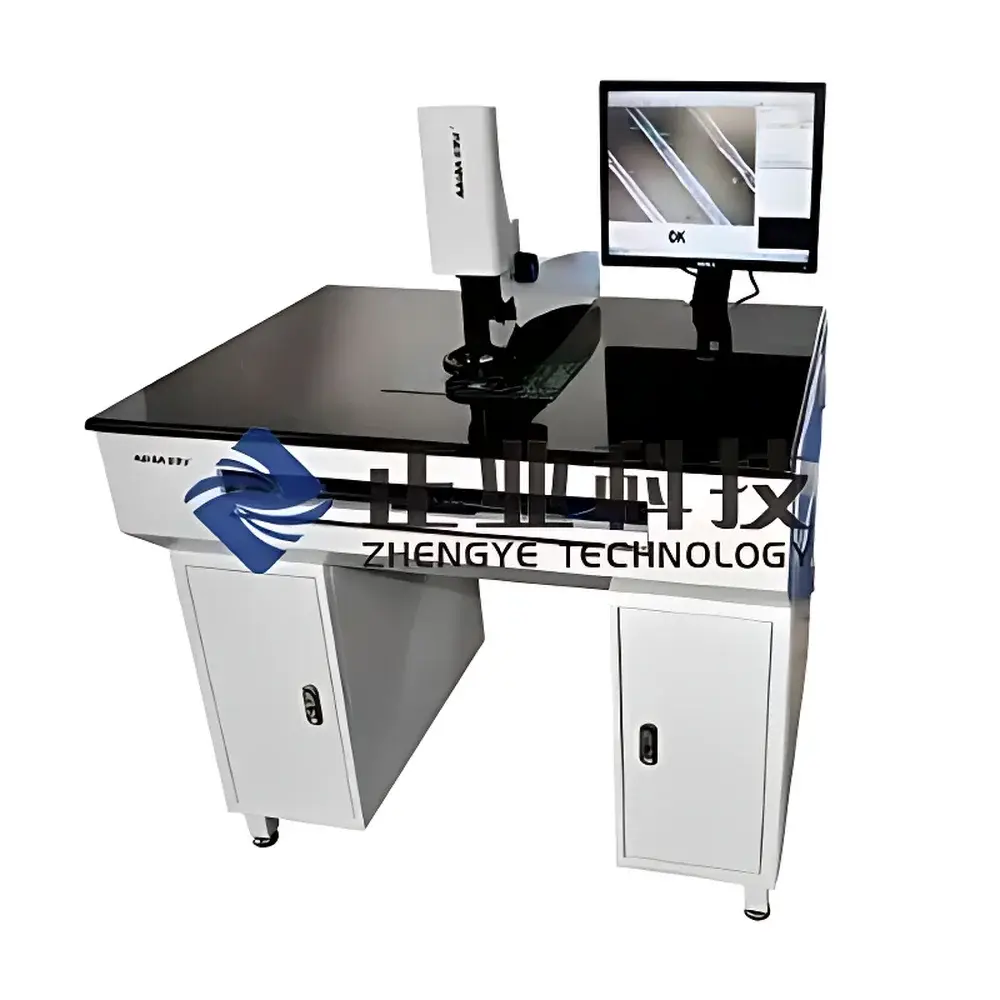
Isida XK22 Benchtop Line Width Measurement System
| [Brand | Isida |
|---|---|
| Origin | Guangdong, China |
| Model | XK22 |
| Resolution | 0.70–5.20 µm/pixel |
| Optical Magnification | 1.4×–9× (continuously adjustable) |
| Electronic Magnification | 50× |
| Light Source | Adjustable LED ring light + red laser diode (LD) positioning |
| CCD | High-sensitivity color CCD |
| Maximum PCB width | 780 mm (30") |
| Field of View | 3.4 mm × 2.5 mm to 0.53 mm × 0.4 mm |
| Repeatability | ±1 µm |
| Dimensions (L×W×H, instrument only) | 960 mm × 700 mm × 1220 mm |
| Weight (instrument only) | 145 kg |
| Power | 220 V ±10%, 50 Hz, 10 A |
| Operating Temperature | 0–40 °C] |
Overview
The Isida XK22 Benchtop Line Width Measurement System is a precision optical metrology instrument engineered for non-contact, high-resolution dimensional analysis of conductive traces and micro-features on printed circuit boards (PCBs), semiconductor wafers, LCD substrates, and thin-film photomasks. It operates on the principle of digital image-based edge detection: a calibrated optical path—comprising continuously variable zoom optics, high-uniformity LED ring illumination, and a red laser diode (LD) crosshair—projects magnified, diffraction-limited images onto a high-sensitivity color CCD sensor. The resulting digital image is processed in real time using sub-pixel interpolation algorithms to determine trace widths (top and bottom profiles), hole diameters (through-holes, blind vias), line-to-line spacing, and corner geometry with traceable repeatability of ±1 µm. Designed specifically for post-etch, pre-solder-mask process control in PCB fabrication, the system meets the geometric verification requirements defined in IPC-6012, IPC-A-600, and JIS C 5012 standards.
Key Features
- Continuously adjustable optical magnification (1.4×–9×) paired with 50× electronic zoom enables flexible field-of-view selection—from macro inspection (3.4 mm × 2.5 mm) down to high-resolution micro-measurement (0.53 mm × 0.4 mm) without lens swapping.
- High-sensitivity color CCD delivers high signal-to-noise ratio imaging under low-light conditions; supports RGB channel separation for contrast-optimized edge detection on varied substrate finishes (e.g., bare copper, electroplated tin, OSP-coated surfaces).
- Dual independent light control: adjustable-intensity LED ring light for uniform oblique illumination (critical for top/bottom width differentiation), and a Class II red LD pointer for rapid ROI localization—reducing setup time by >40% compared to manual stage positioning.
- Motorized coarse/fine Z-axis focusing mechanism ensures consistent depth-of-field alignment across large-format PCBs (up to 780 mm wide); mechanical stability maintained via granite base and vibration-damped column assembly.
- Role-based software interface with administrator and operator modes supports ISO/IEC 17025-compliant audit trails: all measurement parameters, user logins, calibration events, and report exports are timestamped and digitally signed.
Sample Compatibility & Compliance
The XK22 accommodates rigid and flex PCBs (FR-4, polyimide, metal-core), silicon wafers (up to 8″), glass LCD panels, and photomask blanks. Its open-stage design allows direct placement of panelized or depanelized substrates up to 780 mm × 600 mm. All optical and mechanical components comply with IEC 61000-6-2 (EMC immunity) and IEC 61000-6-4 (EMC emission) standards. Measurement uncertainty is validated per ISO 15530-3 (coordinate measuring machines) using NIST-traceable step gauges and line-width standards (e.g., NIST SRM 2053). Software supports export of measurement data in CSV, XML, and PDF formats compliant with FDA 21 CFR Part 11 for electronic records and signatures in regulated environments.
Software & Data Management
The proprietary Isida MetroVision™ software features automated edge detection using adaptive thresholding and second-derivative (Laplacian-of-Gaussian) contour tracing—capable of resolving asymmetric sidewalls and tapered profiles common in etch-defined traces. Each measurement session generates an immutable metadata package including image capture timestamp, optical settings, user ID, environmental temperature/humidity logs (via optional external sensor integration), and full audit trail. Reports conform to IPC-2221B Annex D templates and support SPC charting (X̄-R, Cp/Cpk) directly within the GUI. Data export is configurable for MES integration via OPC UA or RESTful API endpoints; raw TIFF images and calibrated coordinate lists are stored in hierarchical folder structures with SHA-256 checksums for long-term integrity verification.
Applications
- PCB manufacturing: Top/bottom line width verification after pattern plating and etching; solder mask registration accuracy; annular ring assessment for via reliability.
- Semiconductor packaging: Bond pad width and pitch measurement on leadframes and organic substrates; die attach land geometry validation.
- Display technology: TFT array line width uniformity on Gen 2–Gen 4 glass substrates; black matrix opening dimensional control.
- Advanced packaging: Redistribution layer (RDL) trace profiling; fan-out wafer-level packaging (FOWLP) bump pitch and coplanarity analysis.
- Quality assurance labs: First-article inspection (FAI) per AS9102; internal calibration verification against master artifacts; Gage R&R studies per AIAG MSA v4.
FAQ
What is the minimum measurable line width supported by the XK22?
The effective resolution is 0.70 µm/pixel at maximum optical magnification. With sub-pixel edge interpolation, nominal line widths ≥2.5 µm can be measured with ≤±1 µm repeatability under controlled lab conditions (23 ±1 °C, ISO Class 7 cleanroom air).
Does the system support automatic batch measurement of multiple identical features?
Yes—MetroVision™ includes template-based auto-location: users define one reference feature, then apply pattern matching across the entire field or across multiple positions using programmable XY stage coordinates (optional motorized stage required).
Is calibration traceable to national metrology institutes?
All factory calibrations use NIST-traceable line-width standards (SRM 2053) and certified step-height gauges. A full calibration certificate—including uncertainty budget per GUM (JCGM 100:2008)—is provided with each instrument shipment.
Can the software generate SPC-compliant control charts?
Yes—real-time X̄-R, individual/moving range (I-MR), and capability indices (Cp, Cpk, Pp, Ppk) are computed automatically from measurement series and exported as interactive HTML reports with statistical process limits.
What maintenance is required to sustain measurement accuracy?
Annual recalibration is recommended. Daily verification uses built-in check standards (10 µm and 50 µm line-width targets); optical path cleanliness and LED intensity drift are monitored via integrated photometric diagnostics in the software’s maintenance dashboard.


