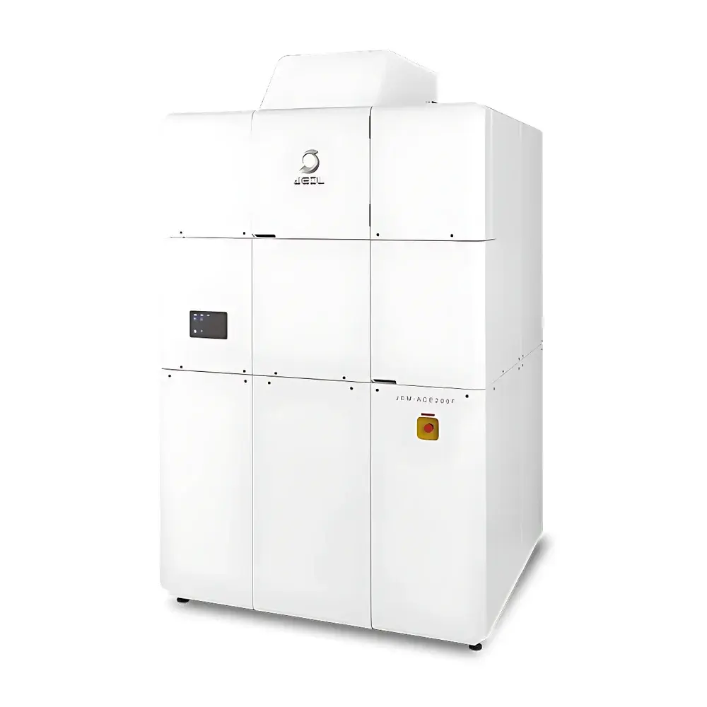
JEOL JEM-ACE200F High-Throughput Field-Emission Transmission Electron Microscope
| Brand | JEOL |
|---|---|
| Origin | Japan |
| Manufacturer Type | Authorized Distributor |
| Product Origin | Imported |
| Model | JEM-ACE200F |
| Price | USD $3,000,000 |
| Acceleration Voltage | Up to 200 kV |
| Maximum Magnification | 2,000,000× |
| Point Resolution | 0.21 nm |
| Lattice Resolution | 0.10 nm |
| STEM Resolution | 0.136 nm |
| Information Limit | 0.11 nm |
| EDS Configuration | Dual Ultra-High-Sensitivity Silicon Drift Detectors (SDD) |
| Lorentz Mode | Standard |
Overview
The JEOL JEM-ACE200F is a purpose-engineered high-throughput field-emission transmission electron microscope (FE-TEM) designed for laboratories requiring both atomic-scale structural fidelity and rapid, reproducible analytical throughput. Operating at a maximum acceleration voltage of 200 kV, the system leverages a cold-field emission gun (CFEG) to deliver exceptional beam coherence, stability, and brightness—critical prerequisites for high-resolution imaging, quantitative electron energy-loss spectroscopy (EELS), and nanoscale elemental mapping. Its architecture integrates advanced aberration-stable lens design, active vibration and acoustic isolation, and electromagnetic interference (EMI)-resilient housing—features directly addressing operational challenges in shared core facilities and industrial R&D environments where ambient stability cannot be guaranteed. Unlike conventional TEM platforms, the ACE200F adopts a reconfigured mechanical layout and compact, shielded column envelope that minimizes sensitivity to floor vibrations and stray magnetic fields, enabling consistent sub-angstrom performance without requiring dedicated basement-level infrastructure.
Key Features
- Atomic-resolution imaging capability: 0.21 nm point resolution and 0.10 nm lattice resolution under standard operating conditions, verified per ISO 16174:2015 for electron optical instruments.
- Sub-nanometer scanning transmission electron microscopy (STEM): Achieves 0.136 nm probe size with high-current, high-coherence illumination—optimized for annular dark-field (ADF) imaging and simultaneous multi-detector EDS acquisition.
- Dual ultra-sensitive silicon drift detector (SDD) configuration: Enables high-count-rate, low-noise energy-dispersive X-ray spectroscopy (EDS) with <125 eV Mn-Kα energy resolution at 100,000 cps, supporting quantifiable elemental mapping at ≤1 nm spatial sampling.
- Integrated Lorentz mode: Standard configuration supports in-focus magnetic domain imaging and off-axis electron holography without hardware modification—essential for characterizing magnetic nanostructures, spintronic materials, and topological defects.
- Automated workflow engine: Includes intelligent stage navigation, auto-focus/astigmatism correction, beam tilt alignment, and recipe-driven acquisition sequences compliant with GLP documentation requirements.
- Modular column architecture: Facilitates rapid in-situ upgrades—including cryo-transfer systems, heating/cooling holders, and in situ biasing stages—without vacuum break or realignment.
Sample Compatibility & Compliance
The JEM-ACE200F accommodates standard 3 mm TEM grids (including SiN membrane, carbon lace, and holey carbon variants) and supports specialized holders for in situ electrical, thermal, and mechanical testing. Specimen insertion uses a dual-airlock loading system with pressure interlocks and bake-out capability up to 120 °C, ensuring ultra-high vacuum integrity (<2 × 10⁻⁸ Pa base pressure). The platform complies with IEC 61000-6-3 (EMC emissions) and IEC 61000-6-2 (immunity), and its software architecture meets FDA 21 CFR Part 11 requirements for electronic records and signatures when deployed with JEOL’s optional Audit Trail and User Access Control modules. All calibration procedures adhere to ASTM E1199-22 (Standard Practice for Calibration of Transmission Electron Microscopes).
Software & Data Management
Control and analysis are performed via JEOL’s ACE-Studio™ suite—a 64-bit, multi-threaded application built on Qt framework and optimized for Windows 10/11 LTSB environments. The software provides synchronized acquisition across imaging, diffraction, EDS, and EELS channels; supports HDF5-based data storage for metadata-rich, FAIR-compliant datasets; and includes batch processing pipelines for automated particle picking, crystallographic orientation mapping (ASTAR), and spectral deconvolution using non-negative matrix factorization (NMF). Raw image and spectrum data export conforms to EMDB/EMPIAR deposition standards. Optional integration with LabArchives ELN enables direct experimental metadata linkage and version-controlled report generation.
Applications
The JEM-ACE200F serves as a primary characterization tool in advanced materials development (e.g., battery cathode interfaces, 2D heterostructures, and catalyst nanoparticles), semiconductor process control (gate oxide integrity, defect tomography), pharmaceutical solid-state analysis (polymorph identification, amorphous content assessment), and life sciences (cryo-ET subtomogram averaging, metal-labeled protein complexes). Its high beam stability and dual-EDS configuration make it particularly suited for statistically robust compositional profiling of heterogeneous catalysts and grain boundary segregation studies in high-entropy alloys.
FAQ
Is the JEM-ACE200F compatible with cryogenic TEM workflows?
Yes—the system supports optional Gatan 626/914 cryo-transfer holders and integrates with JEOL’s Cryo-ACE cooling module for stable operation below −180 °C.
Can the dual-EDS configuration be used for quantitative thin-film analysis?
Yes—when combined with Cliff-Lorimer or ζ-factor standards and thickness maps derived from log-ratio EELS, the system delivers ±3% relative accuracy for films ≥5 nm thick.
Does Lorentz mode require additional lenses or apertures?
No—Lorentz imaging is enabled via dedicated lens excitation modes within the objective lens system; no hardware changes are needed.
What level of service support is available outside Japan?
JEOL provides global coverage through certified regional service centers, including annual preventive maintenance contracts, remote diagnostics, and on-site engineer dispatch within 72 business hours under Platinum Support agreements.


