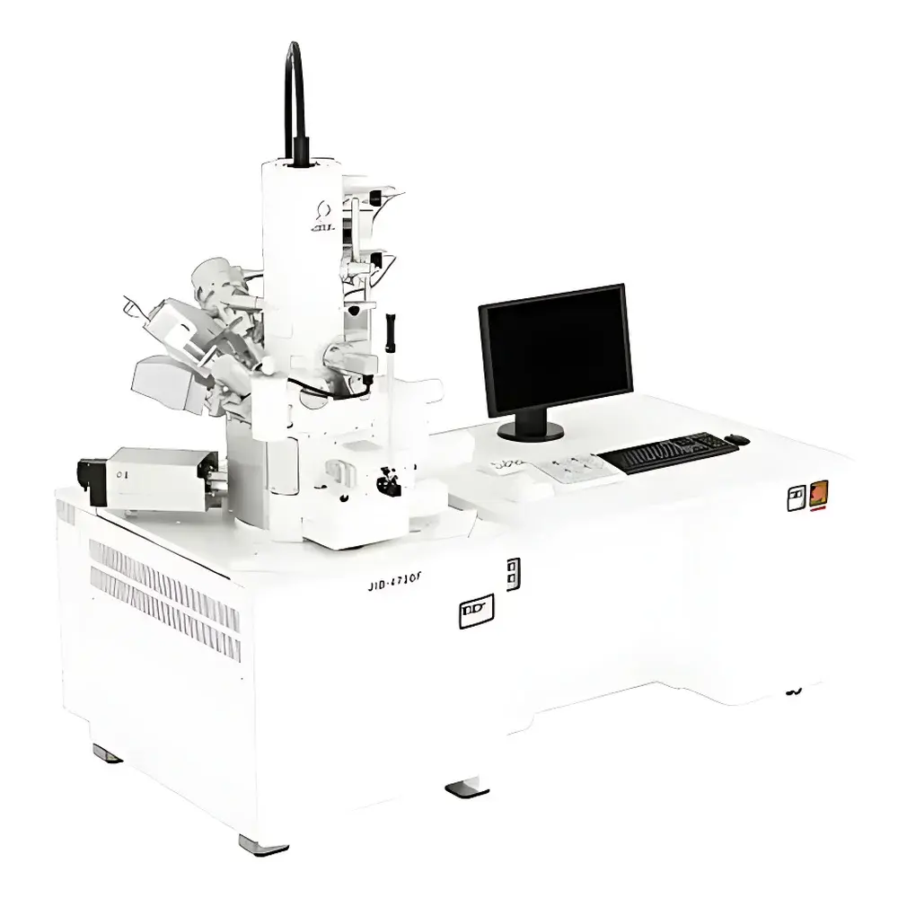
JEOL JIB-4700F Dual-Beam Focused Ion Beam Scanning Electron Microscope
| Brand | JEOL |
|---|---|
| Origin | Japan |
| Model | JIB-4700F |
| Instrument Type | Benchtop Dual-Beam FIB-SEM |
| Electron Source | Cold Field Emission Gun (CFEG) |
| Secondary Electron Resolution | 1.2 nm @ 15 kV, 1.6 nm @ 1 kV |
| Backscattered Electron Resolution | 2.5 nm |
| FIB Resolution | 5 nm @ 30 kV |
| Magnification Range | 25× – 1,000,000× |
| Acceleration Voltage | 0.1–30 kV |
| Maximum FIB Current | 90 nA |
| Maximum SEM Probe Current | 300 nA |
| Gas Injection System | Up to 3 independent channels |
| Sample Stage | 5-axis fully aligned motorized stage |
| Maximum Sample Diameter | 150 mm |
| Sample Loading | Airlock-style exchange |
| Detector Interfaces | EDS, EBSD, STEM, SE/BSE |
Overview
The JEOL JIB-4700F is a high-performance dual-beam focused ion beam–scanning electron microscope (FIB-SEM) engineered for nanoscale characterization, precision site-specific milling, and in situ structural analysis. Unlike conventional single-beam instruments, the JIB-4700F integrates a cold field emission electron gun (CFEG) and a liquid metal ion source (LMIS) gallium ion column into a single, compact benchtop platform—enabling simultaneous or sequential electron imaging, ion beam sputtering, gas-assisted etching/deposition, and tomographic reconstruction. Its optical architecture is optimized for low-voltage SEM imaging with sub-nanometer resolution and high-current FIB operation up to 90 nA, supporting both high-throughput cross-sectioning and fine-feature nanofabrication. Designed for materials science laboratories, semiconductor failure analysis labs, and academic nanotechnology centers, the system delivers quantitative structural and compositional data under controlled vacuum conditions compliant with ISO 14644-1 Class 5 cleanroom integration standards.
Key Features
- Cold field emission electron source delivering exceptional brightness and long-term probe stability—critical for high-resolution imaging at low accelerating voltages (down to 1 kV) without significant charging artifacts.
- Dual-column geometry with precisely aligned electron and ion optical axes, enabling real-time correlation between SEM observation and FIB modification during milling, lift-out, or TEM lamella preparation.
- High-current FIB capability (up to 90 nA) combined with variable spot size control for rapid material removal and fine-tuning of milling depth and edge quality.
- Integrated multi-channel gas injection system (GIS) supporting reactive etching (e.g., XeF2), insulator deposition (e.g., Pt/C), and conductive metal deposition—enabling in situ circuit edit, mask repair, and protective layer formation.
- Airlock-style sample loading mechanism minimizing chamber venting cycles and maintaining base pressure below 1 × 10⁻⁴ Pa during routine operation.
- Five-axis motorized, fully aligned sample stage with sub-micron positional repeatability—supporting tilt-series acquisition for electron tomography and precise alignment of regions-of-interest across multiple modalities.
- Modular detector interface architecture compatible with energy-dispersive X-ray spectroscopy (EDS), electron backscatter diffraction (EBSD), STEM-in-SEM, and segmented BSE/SE detectors—facilitating correlative microstructural and crystallographic analysis.
Sample Compatibility & Compliance
The JIB-4700F accommodates samples up to 150 mm in diameter and 50 mm in height, including wafers, polished cross-sections, biological resin-embedded specimens, and MEMS devices. Its airlock loading system supports rapid sample exchange without breaking high vacuum, reducing downtime between analyses. The instrument meets electromagnetic compatibility (EMC) requirements per IEC 61326-1 and conforms to safety standards outlined in IEC 61010-1 for laboratory electrical equipment. Data acquisition workflows are configurable to support GLP/GMP-compliant environments, with optional audit trail logging and user access controls aligned with FDA 21 CFR Part 11 principles when integrated with JEOL’s SmartSEM software suite.
Software & Data Management
Operation is managed through JEOL’s SmartSEM platform—a Windows-based application offering intuitive workflow automation, scriptable acquisition sequences, and synchronized dual-beam control. The software supports automated lamella thinning protocols, serial sectioning routines for 3D reconstruction, and batch EDS mapping with quantifiable elemental distribution overlays. Raw image and spectrum data are stored in vendor-neutral formats (e.g., TIFF, .emsa, .hdf5), ensuring interoperability with third-party analysis tools such as Thermo Fisher Avizo, Oxford AZtec, or MATLAB-based reconstruction pipelines. All session metadata—including beam parameters, stage coordinates, GIS gas flow rates, and timestamped operator actions—are embedded in image headers for full traceability.
Applications
- Failure analysis of advanced nodes (<10 nm) in logic and memory ICs, including gate oxide defect localization, via stub inspection, and interconnect void detection.
- Preparation of electron-transparent TEM specimens from bulk materials, thin films, and heterostructures—with minimal amorphization and ion implantation artifacts.
- In situ nanomechanical testing using micropillar compression, where FIB-machined pillars are imaged and deformed inside the chamber while monitoring deformation via high-speed SEM.
- 3D microstructure reconstruction of battery cathode particles, catalyst agglomerates, and geological inclusions via FIB-SEM serial sectioning and volume rendering.
- Microfabrication of photonic crystals, plasmonic nanoantennas, and fluidic nanochannels requiring sub-10 nm feature fidelity and multi-material selectivity.
FAQ
What is the minimum detectable feature size achievable with the JIB-4700F in FIB mode?
The system achieves a nominal FIB resolution of 5 nm at 30 kV under optimal conditions; actual feature fidelity depends on material sputter yield, beam dwell time, and gas-assisted chemistry.
Can the JIB-4700F perform automated EBSD mapping in conjunction with FIB milling?
Yes—when equipped with an EBSD detector and configured with SmartSEM’s integrated scripting engine, users can define region-specific milling followed by automated crystallographic orientation mapping.
Is the gas injection system compatible with non-standard precursor gases?
The standard GIS supports three independently controlled channels with calibrated mass flow controllers; custom precursors may be introduced subject to chemical compatibility verification with JEOL engineering support.
Does the system support remote operation and monitoring?
Remote desktop access and live image streaming are supported via secure LAN/WAN connections; however, beam-sensitive operations require local network latency <50 ms for stable control.
What vacuum level is maintained during extended FIB operation?
The differential pumping architecture maintains a specimen chamber pressure of ≤2 × 10⁻⁴ Pa during continuous ion beam exposure, minimizing Ga+ contamination and secondary electron signal degradation.


