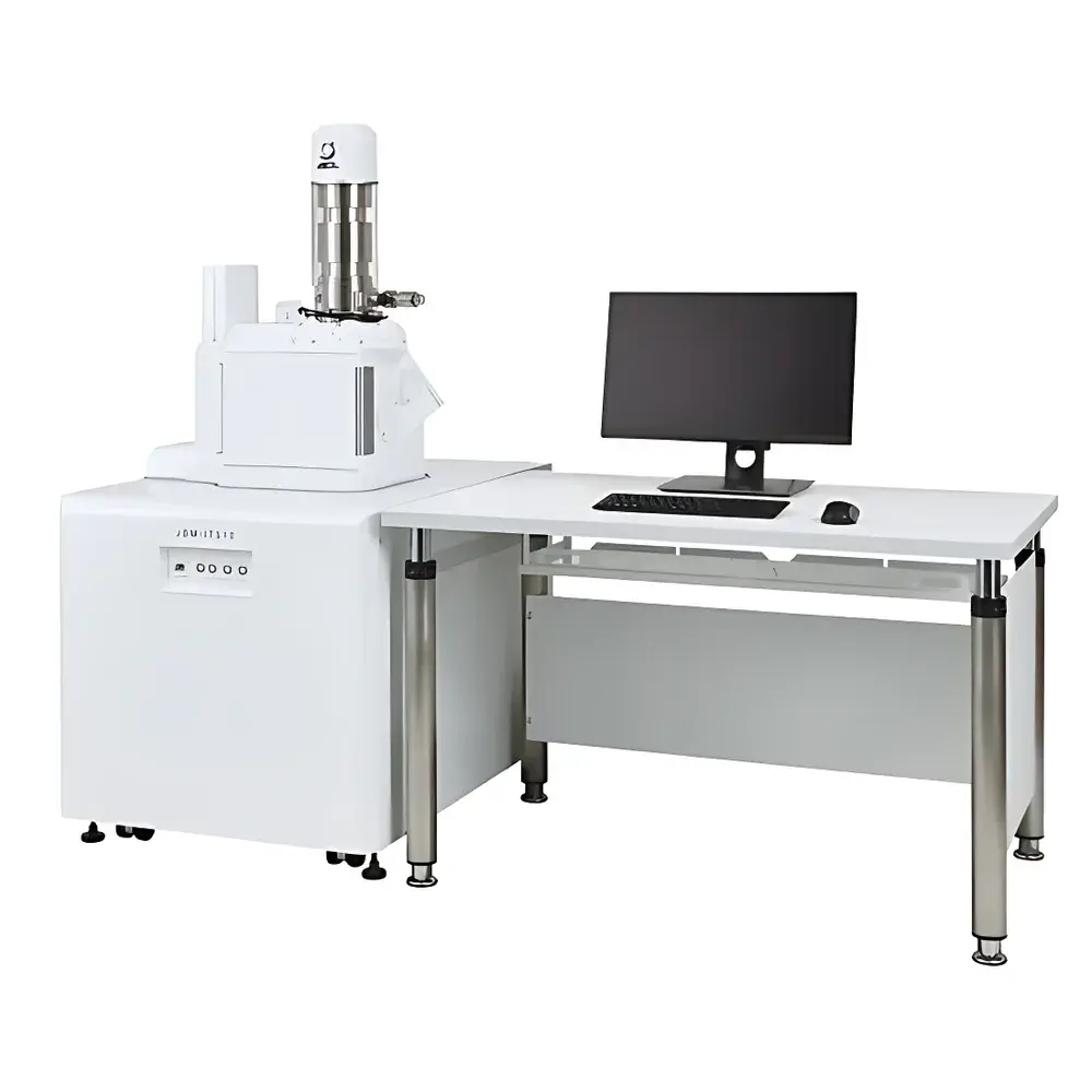
JEOL JSM-IT510 Tungsten-Filament Scanning Electron Microscope
| Brand | JEOL |
|---|---|
| Origin | Japan |
| Model | JSM-IT510 |
| Instrument Type | Floor-standing SEM |
| Electron Source | Tungsten Filament |
| Secondary Electron Resolution | 3 nm @ 30 kV, 15 nm @ 1 kV |
| Backscattered Electron Resolution | 4 nm @ 30 kV |
| Accelerating Voltage Range | 0.3–30 kV |
| Magnification Range | 14×–800,000× (on display) |
| Vacuum Mode | Low-vacuum compatible with LHSED detector |
Overview
The JEOL JSM-IT510 is a floor-standing tungsten-filament scanning electron microscope engineered for high-reproducibility imaging and integrated elemental analysis in routine laboratory environments. Designed around a robust thermionic emission electron source, the system operates across a wide accelerating voltage range (0.3–30 kV), enabling flexible optimization for both conductive and moderately non-conductive samples without mandatory metal coating. Its optical architecture employs a multi-lens column with optimized stigmator and beam alignment systems to ensure stable probe formation and consistent signal collection—critical for quantitative morphology assessment and comparative microstructural studies. The JSM-IT510 was introduced globally in November 2021 as an evolution of JEOL’s established IT-series platform, incorporating enhancements in user workflow efficiency, low-vacuum performance, and real-time analytical synergy between imaging and energy-dispersive X-ray spectroscopy (EDS).
Key Features
- Integrated Low-Vacuum High-Sensitivity Secondary Electron Detector (LHSED): Enables simultaneous detection of secondary electrons and cathodoluminescence photons under low-vacuum conditions (up to 130 Pa), improving signal-to-noise ratio for topographic contrast on uncoated or beam-sensitive specimens.
- Real-Time EDS Integration: Synchronized acquisition of SEM images and EDS spectra allows immediate elemental mapping and point analysis during observation—no post-acquisition correlation required.
- Live 3D Surface Reconstruction: Utilizes stereo-pair imaging and depth-from-shading algorithms to generate interactive 3D surface models directly from standard SE/BSE acquisitions, supporting qualitative depth perception and geometric interpretation of rough or layered structures.
- Smart Navigation Zoom Functionality: Provides a 4× optical-microscope-equivalent overview image prior to high-magnification scanning, facilitating rapid region-of-interest selection and seamless transition from macro- to micro-scale inspection.
- Zero-Magnification Mode: Allows direct overlay of optical-level field-of-view markers onto the SEM stage coordinate system, enabling precise relocation of multiple sites across sessions without manual recalibration.
- X-ray Generation Zone Visualization: Graphically overlays the estimated interaction volume (based on acceleration voltage and material Z-number) onto the displayed image, aiding interpretation of analysis depth and potential matrix effects in EDS quantification.
Sample Compatibility & Compliance
The JSM-IT510 accommodates a broad spectrum of solid-state specimens—including metals, ceramics, polymers, geological sections, biological tissues (fixed or freeze-dried), and composite materials—without requiring conductive coating in many cases, thanks to its low-vacuum operation and charge-compensation capabilities. Specimen dimensions up to Ø100 mm × 50 mm height are supported using standard stubs and tilt/rotation stages. The system complies with IEC 61000-6-3 (EMC emissions) and IEC 61000-6-2 (immunity) standards. While not inherently 21 CFR Part 11 compliant out-of-the-box, SMILE VIEW™ Lab software supports audit-trail-enabled report generation when deployed within validated laboratory information management systems (LIMS) adhering to GLP/GMP frameworks.
Software & Data Management
SMILE VIEW™ Lab serves as the unified interface for instrument control, image acquisition, EDS data processing, and report compilation. It supports DICOM-compatible metadata embedding, TIFF/PNG export with embedded scale bars and acquisition parameters, and batch-processing workflows for standardized imaging protocols. All acquired images and spectral datasets are stored with timestamped metadata, including kV, working distance, dwell time, detector type, and vacuum status. The software permits user-defined template-based reporting, with automated inclusion of annotated images, elemental maps, line scans, and summary tables—facilitating compliance with internal SOPs and external quality assurance requirements such as ISO/IEC 17025.
Applications
The JSM-IT510 is routinely deployed in materials science laboratories for failure analysis of electronic components, fracture surface characterization in metallurgy, porosity and particle size distribution assessment in catalysts and pharmaceutical excipients, and morphological evaluation of nanocomposites. In academic research, it supports teaching of electron-solid interactions, undergraduate microscopy labs, and preliminary screening prior to high-resolution TEM or FIB-SEM investigation. Industrial QA/QC applications include incoming raw material verification, coating thickness estimation via cross-section imaging, and contamination identification in semiconductor packaging environments.
FAQ
What vacuum modes does the JSM-IT510 support?
The system operates in high vacuum (HV) mode for maximum resolution on conductive samples and low vacuum (LV) mode (up to 130 Pa) for enhanced charge dissipation on insulators.
Is EDS hardware included as standard equipment?
Yes—the JSM-IT510 is shipped with a silicon drift detector (SDD)-based EDS system fully integrated into the column and software interface.
Can the system be upgraded to field emission capability?
No—this model utilizes a tungsten thermionic source; field emission upgrades require replacement with a dedicated FE-SEM platform such as the JSM-IT800 series.
Does SMILE VIEW™ Lab support automated particle analysis?
Basic particle counting and sizing functions are available via threshold-based segmentation tools; advanced AI-driven classification requires third-party plugin integration.
What is the typical service life of the tungsten filament?
Under standard operating conditions (30 kV, 10–30 µA emission current), filament lifetime averages 100–150 hours, with automatic filament alignment and emission tuning reducing operator dependency.


