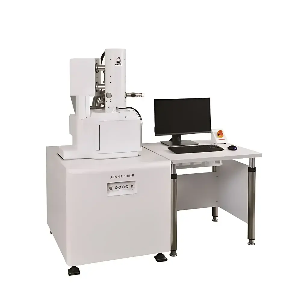
JEOL JSM-IT710HR InTouchScope™ Thermal Field Emission Scanning Electron Microscope
| Brand | JEOL |
|---|---|
| Origin | Japan |
| Model | JSM-IT710HR |
| Instrument Type | Benchtop SEM |
| Electron Source | Thermal Field Emission Gun (TFEG) |
| Secondary Electron Resolution | 1 nm @ 30 kV |
| Backscattered Electron Resolution | 2 nm @ 30 kV |
| Accelerating Voltage | 0.1–30 kV |
| Maximum Magnification | 1,000,000× |
| Probe Current | Up to 300 nA |
| Sample Chamber | Large-volume, front-loading with wide-access door |
| Operating Modes | High Vacuum / Low Vacuum (LV/LA variants available) |
Overview
The JEOL JSM-IT710HR InTouchScope™ is a benchtop thermal field emission scanning electron microscope engineered for high-resolution imaging, quantitative elemental analysis, and routine materials characterization in academic, industrial, and quality control laboratories. Utilizing an immersion-type thermal field emission electron gun (TFEG), the system delivers exceptional beam brightness and stability—enabling sub-nanometer secondary electron resolution (1 nm at 30 kV) and high-current probe operation (up to 300 nA) without compromising longevity or vacuum integrity. Unlike cold field emitters, the TFEG offers superior emission stability under variable operating conditions and reduced sensitivity to residual gas contamination, making it ideal for environments where rapid sample turnover and multi-user access are standard practice. The JSM-IT710HR integrates a compact, vibration-damped mechanical architecture with a large-volume sample chamber and front-access door—supporting specimens up to 150 mm in diameter and 80 mm in height—while maintaining rigorous alignment repeatability across voltage and magnification ranges.
Key Features
- InTouchScope™ touch-enabled GUI: Intuitive, icon-driven interface with gesture support for focus, stigmation, contrast/brightness, and stage navigation—designed for minimal training overhead and consistent operator performance.
- Signal Depth Display: Real-time visualization of effective interaction volume as a function of accelerating voltage and material composition—critical for optimizing EDS acquisition geometry and interpreting quantification accuracy.
- Zeromag optical-electron correlation: Integrated wide-field optical camera enables seamless transition from macroscopic overview to high-magnification SEM imaging; coordinates are automatically registered between optical and electron frames.
- Live Analysis mode: Synchronous acquisition of secondary electron (SE), backscattered electron (BSE), and energy-dispersive X-ray (EDS) spectra during stage movement—enabling rapid compositional screening without interrupting navigation.
- 3D Live Image: Real-time stereo reconstruction from dual BSE detectors with dynamic tilt compensation—generating topographic maps without mechanical stage tilting or post-acquisition processing.
- SMILE VIEW™ Lab software suite: Unified platform for image annotation, measurement, EDS point/line/map quantification, report generation (PDF/HTML), and audit-trail-compliant data export per ISO/IEC 17025 and GLP requirements.
- Automated beam alignment & stigmation: On-the-fly correction routines maintain optimal probe shape and current density across voltage sweeps and working distance adjustments.
Sample Compatibility & Compliance
The JSM-IT710HR accommodates conductive, semi-conductive, and non-conductive specimens—including bulk metals, polished cross-sections, powders, biological tissues (with optional low-vacuum mode), and coated polymers—without mandatory sputter coating in many cases. Its dual-mode vacuum system supports both high-vacuum operation (≤1.0 × 10⁻⁴ Pa) for maximum resolution and low-vacuum mode (10–133 Pa) for charge-free imaging of insulating samples. The instrument complies with IEC 61000-6-3 (EMC emissions), IEC 61000-6-2 (immunity), and meets essential safety requirements per IEC 61010-1. Optional configurations include EDS detectors certified to ASTM E1508 standards for quantitative microanalysis and integrated stage encoders traceable to NIST reference standards.
Software & Data Management
SMILE VIEW™ Lab provides full digital workflow integration—from acquisition through reporting—with built-in metadata tagging (user ID, timestamp, instrument parameters, calibration logs). All raw images and spectral data are stored in vendor-neutral formats (TIFF, .emsa, .msa) alongside XML-based parameter records. Software supports 21 CFR Part 11-compliant user authentication, electronic signatures, and audit trail logging for regulated environments. Remote monitoring and diagnostic capabilities allow service engineers to perform preliminary troubleshooting via secure TLS-encrypted connection—minimizing downtime and supporting preventive maintenance scheduling aligned with ISO 9001 quality management systems.
Applications
The JSM-IT710HR serves core applications across semiconductor process control (defect review, line-width metrology, interconnect inspection), advanced materials R&D (nanoparticle dispersion analysis, grain boundary characterization, thin-film morphology), metallurgy (inclusion analysis, fracture surface evaluation), geosciences (mineral phase mapping), and life sciences (cellular ultrastructure, tissue scaffolds, biomaterial interfaces). Its high probe current and stable TFEG make it particularly suited for time-resolved EDS mapping, low-dose imaging of beam-sensitive specimens, and automated particle analysis workflows compliant with ISO 13322-2.
FAQ
What vacuum modes does the JSM-IT710HR support?
It operates in high vacuum (HV) mode for maximum resolution and low vacuum (LV) mode for uncoated insulators—selectable via software without hardware modification.
Is EDS integration included as standard?
EDS detection is available as a factory-configured option; detector type (Si(Li) or SDD), solid angle, and cooling method are specified at order entry.
Can the system be upgraded for electron backscatter diffraction (EBSD)?
Yes—EBSD compatibility is supported through optional detector mounting kits and software licensing; requires alignment verification per ASTM E1122.
Does the instrument meet regulatory requirements for GMP laboratories?
When configured with Part 11-compliant SMILE VIEW™ Lab and validated installation qualification (IQ/OQ), it fulfills documentation and traceability requirements for pharmaceutical and medical device QA/QC.
What is the typical service interval for the thermal field emitter?
Under normal operating conditions (≤8 h/day, clean vacuum environment), the TFEG maintains stable emission for ≥12 months before scheduled refurbishment—significantly exceeding cold FEG lifetime expectations.


