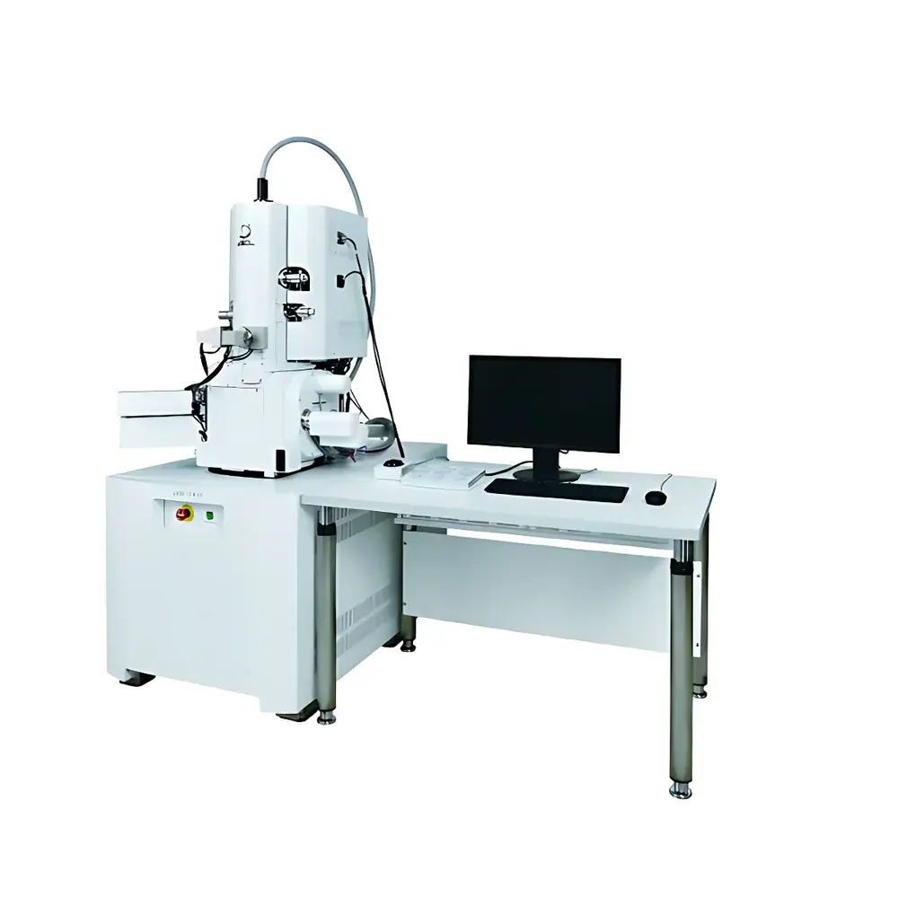
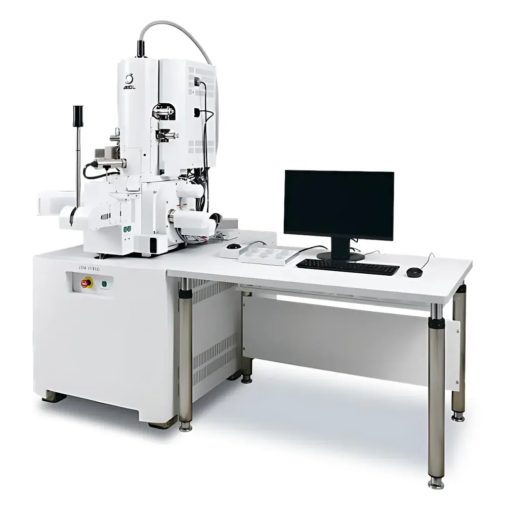
JEOL JSM-IT810 Field Emission Scanning Electron Microscope
| Brand | JEOL |
|---|---|
| Origin | Japan |
| Model | JSM-IT810 |
| Instrument Type | Floor-standing SEM |
| Electron Gun | Thermal Field Emission (TFE) |
| Secondary Electron (SE) Resolution | 0.5 nm at 15 kV |
| Backscattered Electron (BSE) Resolution | 1.5 nm at 15 kV |
| Accelerating Voltage Range | 0.01–30 kV |
| Magnification Range | ×27 to ×5,480,000 (at 1280 × 960 pixels) |
| Beam Current | Up to 500 nA |
| Detector Configuration | Standard In-lens SE, Through-the-lens BSE, and Optional EDS/EBSD Integration |
| Sample Chamber | Expandable with Multiple Ports for In-situ & Analytical Add-ons |
| Stage | Motorized, High-Precision 5-Axis Tilt/Rotation/Translation Stage |
Overview
The JEOL JSM-IT810 is a high-performance, floor-standing field emission scanning electron microscope engineered for nanoscale imaging, compositional analysis, and crystallographic characterization in demanding research and industrial quality control environments. Based on thermal field emission (TFE) electron source technology, the JSM-IT810 delivers exceptional beam stability, high brightness, and sub-nanometer spatial resolution—enabling reliable visualization of surface topography, grain boundaries, phase distribution, and fine structural features across conductive, semi-conductive, and non-conductive specimens. Its immersion-type electron optical column design ensures optimized probe formation over the full accelerating voltage range (0.01–30 kV), supporting low-kV imaging for beam-sensitive materials and high-kV analysis for deep penetration and enhanced signal-to-noise ratio. The platform is purpose-built for multi-modal correlative microscopy, integrating seamlessly with energy-dispersive X-ray spectroscopy (EDS), electron backscatter diffraction (EBSD), cathodoluminescence (CL), and in-situ mechanical or environmental stages.
Key Features
- Thermal field emission (TFE) electron gun delivering stable, high-brightness electron beams up to 500 nA—critical for fast, high-fidelity EDS mapping and quantitative EBSD pattern acquisition.
- Sub-0.5 nm secondary electron (SE) resolution at 15 kV, verified per ISO 16700:2016 standards, with consistent performance across magnifications from ×27 to ×5.48 million.
- Advanced immersion lens architecture enabling simultaneous optimization of resolution, depth of field, and working distance flexibility—ideal for tilted, rough, or height-varied samples.
- Real-time analytical capabilities including live EDS spectrum acquisition, real-time 3D topographic reconstruction via stereo-SEM, and automated drift compensation during long-duration acquisitions.
- Intuitive, icon-driven user interface with guided workflow templates—reducing operator dependency and minimizing training time without compromising analytical rigor.
- Modular chamber design with standardized flange interfaces (CF, ISO-KF) supporting up to eight auxiliary ports for simultaneous detector integration, gas injection systems (GIS), heating/cooling stages, or micro-manipulators.
Sample Compatibility & Compliance
The JSM-IT810 accommodates a broad spectrum of specimen types—including insulating polymers, biological tissues (with optional low-vacuum or cryo-mode), magnetic alloys, ceramic composites, and semiconductor wafers—without mandatory conductive coating in many cases, thanks to its low-voltage imaging capability and charge-compensation modes. All operational parameters are logged with timestamped metadata, satisfying audit requirements under GLP and GMP frameworks. The system complies with IEC 61000-6-3 (EMC emissions) and IEC 61000-6-2 (immunity), and supports 21 CFR Part 11-compliant software configurations when paired with JEOL’s optional SecureSEM™ module for electronic signatures, role-based access control, and immutable audit trails.
Software & Data Management
Acquisition and analysis are managed through JEOL’s proprietary SmartSEM™ software suite, which provides unified control of imaging, stage navigation, detector synchronization, and spectral processing. Raw image data is stored in open-format TIFF or DM3 files; EDS spectra and EBSD patterns adhere to the standardized .eds and .ctf formats for third-party interoperability (e.g., Oxford AZtec, EDAX TEAM™, or Channel5). Batch processing, scripting via Python API, and DICOM export for biomedical applications are fully supported. Data integrity is reinforced through automatic checksum validation, version-controlled project archives, and optional network-attached storage (NAS) integration with RAID redundancy.
Applications
- Nanomaterials characterization: particle size distribution, agglomeration state, and surface functionalization verification.
- Failure analysis in microelectronics: cross-sectional imaging of interconnects, void detection in solder joints, and contamination identification via EDS line scans.
- Metallurgy & additive manufacturing: grain orientation mapping (EBSD), inclusion analysis, and porosity quantification in as-built or heat-treated components.
- Life sciences: high-resolution ultrastructural imaging of freeze-fractured membranes, immunogold labeling, and serial block-face SEM (SBF-SEM) correlation workflows.
- Catalysis & energy materials: catalyst support morphology, pore network analysis, and in-situ electrochemical cell observation under controlled gas environments.
FAQ
What vacuum level does the JSM-IT810 maintain in the electron column and sample chamber?
The electron optical column operates at ultra-high vacuum (UHV) ≤1×10⁻⁷ Pa, while the sample chamber maintains high vacuum ≤1×10⁻⁴ Pa; optional differential pumping enables low-vacuum mode (1–133 Pa) for uncoated insulators.
Is the JSM-IT810 compatible with third-party EDS and EBSD detectors?
Yes—the system features standard detector mounting interfaces and digital trigger synchronization protocols compliant with major vendors (Oxford Instruments, EDAX, Bruker), subject to firmware coordination and physical port availability.
Can the JSM-IT810 perform automated particle analysis (APA) out-of-the-box?
SmartSEM™ includes built-in APA tools for threshold-based segmentation, morphological classification, and statistical reporting; custom algorithms may be deployed via Python scripting.
What stage motion precision and repeatability specifications are guaranteed?
The motorized 5-axis stage offers ±0.1 µm positional repeatability and 0.01° tilt/rotation resolution, calibrated traceably to NIST-traceable interferometric standards.
Does JEOL provide application-specific training and method development support?
Yes—JEOL’s global Application Support Centers offer remote and on-site training, SOP development, and collaborative feasibility studies aligned with ASTM E1558, ISO 16700, and USP guidelines.


