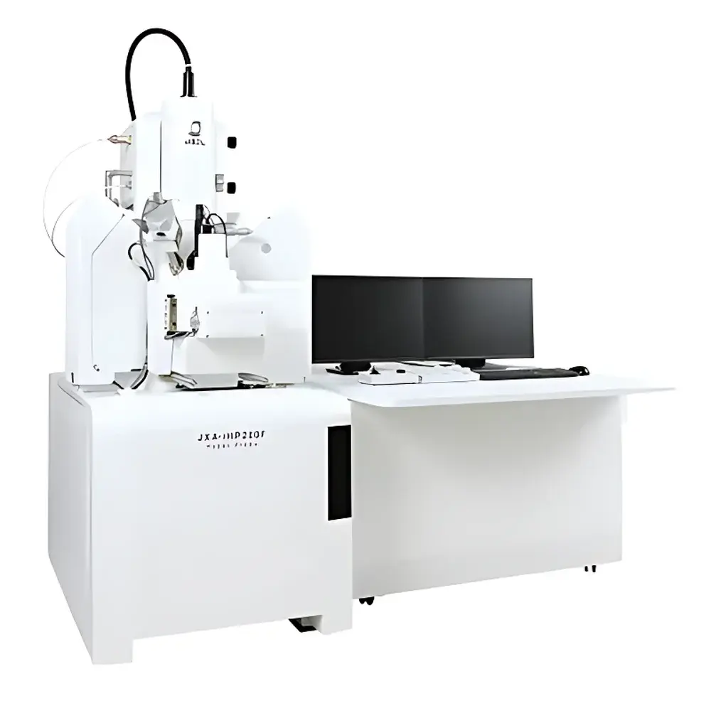
JEOL JXA-iHP200F Field-Emission Electron Probe Microanalyzer (EPMA)
| Brand | JEOL |
|---|---|
| Origin | Japan |
| Model | JXA-iHP200F |
| Instrument Type | Floor-standing, High-Performance EPMA |
| Electron Source | Thermal Field-Emission Gun (TFEG) |
| Secondary Electron Resolution | 2.5 nm at 15 kV |
| Magnification Range | 40× to 300,000× |
| Accelerating Voltage | 1–30 kV |
| Backscattered Electron Imaging | High-Contrast Mode |
| Maximum Sample Dimensions | 100 mm × 100 mm × 50 mm (H) |
| Motorized Stage | 5-Axis Precision Drive |
| Standard Detectors | Solid-State Backscatter Detector, Wavelength-Dispersive Spectrometer (WDS), Energy-Dispersive Spectrometer (EDS) |
| Vacuum System | Ultra-High Vacuum (UHV) Compatible |
| Interface Expansion | Multiple Dedicated Ports for Optional Analyzers (e.g., EBSD, CL, STEM-in-SEM) |
Overview
The JEOL JXA-iHP200F is a high-precision, floor-standing electron probe microanalyzer engineered for quantitative elemental analysis at sub-micrometer spatial resolution. Unlike scanning electron microscopes optimized primarily for imaging, the JXA-iHP200F implements a dedicated electron optical column and ultra-stable beam delivery system designed specifically for wavelength-dispersive spectroscopy (WDS)—the gold standard for accurate, matrix-corrected compositional quantification in solid materials. Its thermal field-emission electron gun delivers exceptional current stability and probe coherence, enabling high-brightness, low-drift microbeam operation essential for repeatable point analysis, line scans, and elemental mapping. The instrument operates under ultra-high vacuum conditions (<1×10⁻⁶ Pa) to minimize contamination and ensure long-term spectral fidelity. With a fully integrated dual-detection architecture—combining high-resolution WDS spectrometers (with multi-crystal configuration) and a high-count-rate silicon drift detector (SDD)-based EDS system—the JXA-iHP200F bridges the gap between analytical rigor and workflow efficiency.
Key Features
- Thermal field-emission electron source providing superior brightness, energy spread 2,000 hours typical)
- Dual-beam capability: simultaneous WDS and EDS acquisition for cross-validated composition data
- Five-axis motorized stage with sub-micron positional repeatability and programmable tilt/rotation for crystallographic alignment
- Modular chamber design featuring multiple standardized ports (ISO-KF 63 and CF 100) for seamless integration of optional detectors—including electron backscatter diffraction (EBSD), cathodoluminescence (CL), and STEM-in-SEM modules
- High-contrast backscattered electron (BSE) imaging with atomic number (Z)-contrast optimization and real-time topographic correction
- Automated spectrometer alignment, peak identification, and ZAF/φ(ρz) matrix correction routines compliant with ISO 14787 and ASTM E1508 standards
Sample Compatibility & Compliance
The JXA-iHP200F accommodates bulk specimens up to 100 mm × 100 mm × 50 mm (height), including polished metallographic mounts, geological thin sections, ceramic cross-sections, and semiconductor wafers. Its robust sample chamber supports conductive and non-conductive samples alike, with optional low-voltage BSE imaging and charge compensation modes. All analytical protocols adhere to internationally recognized metrological frameworks: quantitative WDS analyses follow ISO 22309 (microanalysis of metals), ASTM E1359 (standard practice for EPMA), and USP guidelines for material characterization in regulated environments. Full audit trail functionality, electronic signature support, and 21 CFR Part 11–compliant software architecture are available via optional JEOL Analysis Suite (JAS) GLP/GMP module.
Software & Data Management
Control and analysis are managed through JEOL’s proprietary JAS platform—a Windows-based, multi-threaded application supporting real-time spectrum acquisition, interactive map stitching, phase identification via integrated database correlation (CAMECA SPC and NIST DTSA-II libraries), and automated report generation in PDF/XLS formats. Raw spectral data are stored in vendor-neutral .jepma binary format, fully compatible with third-party processing tools such as Probe for EPMA and CalcZAF. Data integrity is enforced via time-stamped metadata, user-access logging, and version-controlled method files. Networked deployment allows centralized calibration management and remote monitoring across multi-instrument laboratories.
Applications
The JXA-iHP200F serves critical roles in academic research, national metrology institutes, and industrial QA/QC labs where traceable, certified compositional data are required. Typical use cases include: quantitative analysis of inclusion chemistry in aerospace superalloys; phase boundary composition profiling in battery cathode materials; rare-earth element distribution mapping in permanent magnets; oxidation layer stoichiometry in thermal barrier coatings; and certification of reference materials (CRMs) per ISO Guide 35. Its high spatial resolution and detection limits (typically 10–50 ppm for major elements, depending on matrix and count time) make it indispensable for failure analysis, geochronology (e.g., monazite U-Th-Pb dating), and semiconductor defect forensics.
FAQ
What distinguishes EPMA from SEM-EDS for quantitative analysis?
EPMA employs WDS, which offers ~10× better spectral resolution and lower detection limits than EDS—enabling precise separation of overlapping peaks (e.g., S Kα and Pb Mα) and rigorous matrix correction.
Can the JXA-iHP200F perform automated mineral identification?
Yes—when paired with JEOL’s mineral library and automated stage scripting, it executes standardized mineral mode analyses per ASTM D5361, delivering phase ID, modal abundance, and compositional statistics.
Is remote operation supported?
The JAS platform supports secure remote desktop access and scheduled unattended runs, provided network infrastructure complies with institutional IT security policies.
What vacuum level is maintained during analysis?
The column achieves and sustains <5×10⁻⁷ Pa; the sample chamber operates at <1×10⁻⁶ Pa, verified by cold cathode gauge and ion pump status telemetry.
How is beam drift compensated during long-duration mapping?
Real-time drift correction uses fiducial markers and closed-loop stage feedback, with optional beam-blanking synchronization to minimize cumulative positional error.


