Kelvin Probe Force Microscope SKP5050

| Origin | UK |
|---|---|
| Manufacturer Type | Distributor |
| Origin Category | Imported |
| Model | SKP5050 |
| Component Category | Optical Component |
| Spatial Resolution (Scanning Stage) | <317.5 nm |
| Work Function Resolution | <3 meV |
| Sample Size Range | 5–300 mm |
Ask about pricing, availability and specifications.
Overview
The Kelvin Probe Force Microscope SKP5050 is a high-precision, non-contact surface potential mapping instrument engineered for quantitative work function and contact potential difference (CPD) characterization at micro- to macro-scale dimensions. Operating on the principle of vibrating capacitor electrostatic force detection—rooted in the classical Kelvin probe method—the SKP5050 measures local surface potential variations with sub-3 meV energy resolution without physical contact or sample charging. Unlike conventional scanning tunneling or atomic force microscopy techniques, this system relies on capacitive coupling between a conductive, oscillating probe tip and the sample surface under vacuum or ambient conditions, enabling true surface electronic property mapping independent of topography. Its design integrates a robust, low-noise electrostatic detection architecture optimized for long-term stability and high reproducibility—critical for studies in photovoltaics, corrosion science, semiconductor interface engineering, and organic electronics.
Key Features
- Wide-area scanning capability supporting samples from 5 mm to 300 mm in diameter—enabling wafer-level, device-integrated, and heterogeneous material analysis;
- Sub-3 meV work function resolution, achieved via low-drift, high-gain lock-in amplification and temperature-stabilized electronics;
- High-precision motorized scanning stage with positional resolution better than 317.5 nm and repeatability ≤ ±50 nm over full travel;
- Integrated Faraday cage and optically shielded enclosure—designed to attenuate electromagnetic interference (EMI), acoustic noise, and ambient light fluctuations by >60 dB across 1 Hz–1 MHz;
- Modular platform architecture compatible with optional add-ons including photoemission yield spectroscopy (PYS), surface photovoltage (SPV), and time-resolved Kelvin probe modules;
- Passive thermal management and vibration-damped optical table mounting interface to minimize drift during extended acquisition (>8 h continuous scans).
Sample Compatibility & Compliance
The SKP5050 accommodates electrically conductive, semiconductive, and insulating substrates—including Si wafers, ITO/glass, perovskite films, polymer blends, oxide-coated metals, and biological thin films—without requiring metallization or conductive coating. Sample height variation up to ±2 mm is compensated via real-time Z-feedback control. The system complies with ISO/IEC 17025 general requirements for calibration laboratories, and its measurement traceability aligns with NIST SP 260 series standards for surface potential metrology. All hardware and firmware meet CE marking directives for electromagnetic compatibility (2014/30/EU) and low-voltage safety (2014/35/EU). Data acquisition protocols support audit-ready documentation required under GLP and GMP environments when paired with validated software configurations.
Software & Data Management
Control and analysis are performed using SKP Suite v4.x—a Windows-based application developed in accordance with FDA 21 CFR Part 11 requirements for electronic records and signatures. The software provides full instrument control, automated multi-point CPD mapping, batch processing for comparative analysis, and export of calibrated work function values in SI units (eV). Raw signal data (phase, amplitude, DC offset) are stored in HDF5 format with embedded metadata (timestamp, environmental logs, calibration parameters), ensuring FAIR (Findable, Accessible, Interoperable, Reusable) data principles. Integration with MATLAB and Python APIs enables custom algorithm development for machine learning–assisted defect classification or spatial correlation with complementary techniques (e.g., Raman, XPS, or SEM-EDS datasets).
Applications
- Quantitative mapping of work function gradients across heterojunction solar cells to identify interfacial recombination losses;
- In situ monitoring of corrosion initiation and passivation layer evolution on coated alloys under humid or saline exposure;
- Characterization of charge trapping dynamics in gate dielectrics and ferroelectric memory devices;
- Surface dipole distribution analysis in self-assembled monolayers (SAMs) and molecular semiconductor films;
- Correlation of local surface potential with grain boundaries, phase segregation, and defect density in polycrystalline thin-film devices;
- Validation of theoretical models (e.g., DFT-predicted surface dipoles) through experimental CPD quantification.
FAQ
What environmental conditions are required for optimal SKP5050 operation?
Stable ambient temperature (20–25 °C ± 0.5 °C), relative humidity <50% RH, and low-acoustic-noise environment (<45 dB(A)) are recommended. Operation inside a Class 1000 cleanroom or laminar flow hood is advised for ultra-sensitive measurements.
Can the SKP5050 be used under controlled atmosphere or vacuum?
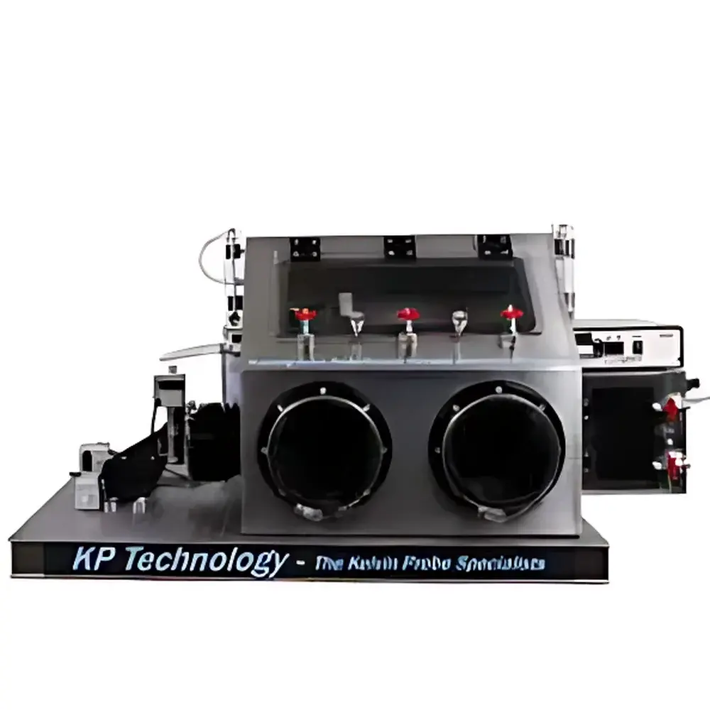
Yes—the probe head and sample stage are compatible with glovebox integration (N₂/Ar) and can be mounted in UHV chambers (≤1×10⁻⁷ mbar) with appropriate feedthroughs and differential pumping.
Is calibration traceable to national standards?
All factory calibrations are referenced to NIST-traceable reference electrodes and certified surface potential standards (e.g., Au(111)/HOPG), with full calibration certificates provided per unit.
How is topographic cross-talk minimized during CPD mapping?
Through dual-channel feedback: simultaneous topographic tracking (via capacitive or optical interferometric Z-servo) decouples vertical motion artifacts from CPD signal acquisition, ensuring <0.5% topography-induced error in work function values.