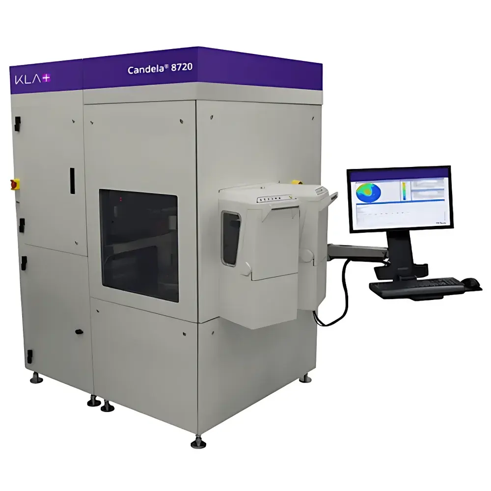
KLA Candela® 8720 Optical Wafer Defect Inspection System
| Brand | KLA-Filmetrics |
|---|---|
| Origin | USA |
| Manufacturer Type | Authorized Distributor |
| Product Category | Imported |
| Model | Candela® 8720 |
| Instrument Type | Optical Patterned Wafer Defect Inspection System |
| Primary Application | Automated wafer inspection with Statistical Process Control (SPC) integration |
| Wafer Diameter | 200 mm |
| Detection Principle | Multi-angle elastic and inelastic scattering imaging |
| Key Capabilities | Simultaneous dual-angle scatterometry, surface topography mapping, reflectance profiling, phase contrast imaging, and photoluminescence (PL) detection |
| Compliance | Designed for semiconductor fab environments compliant with SEMI E30 (SECS/GEM), ISO 9001, and industry-aligned GLP/GMP data integrity expectations |
Overview
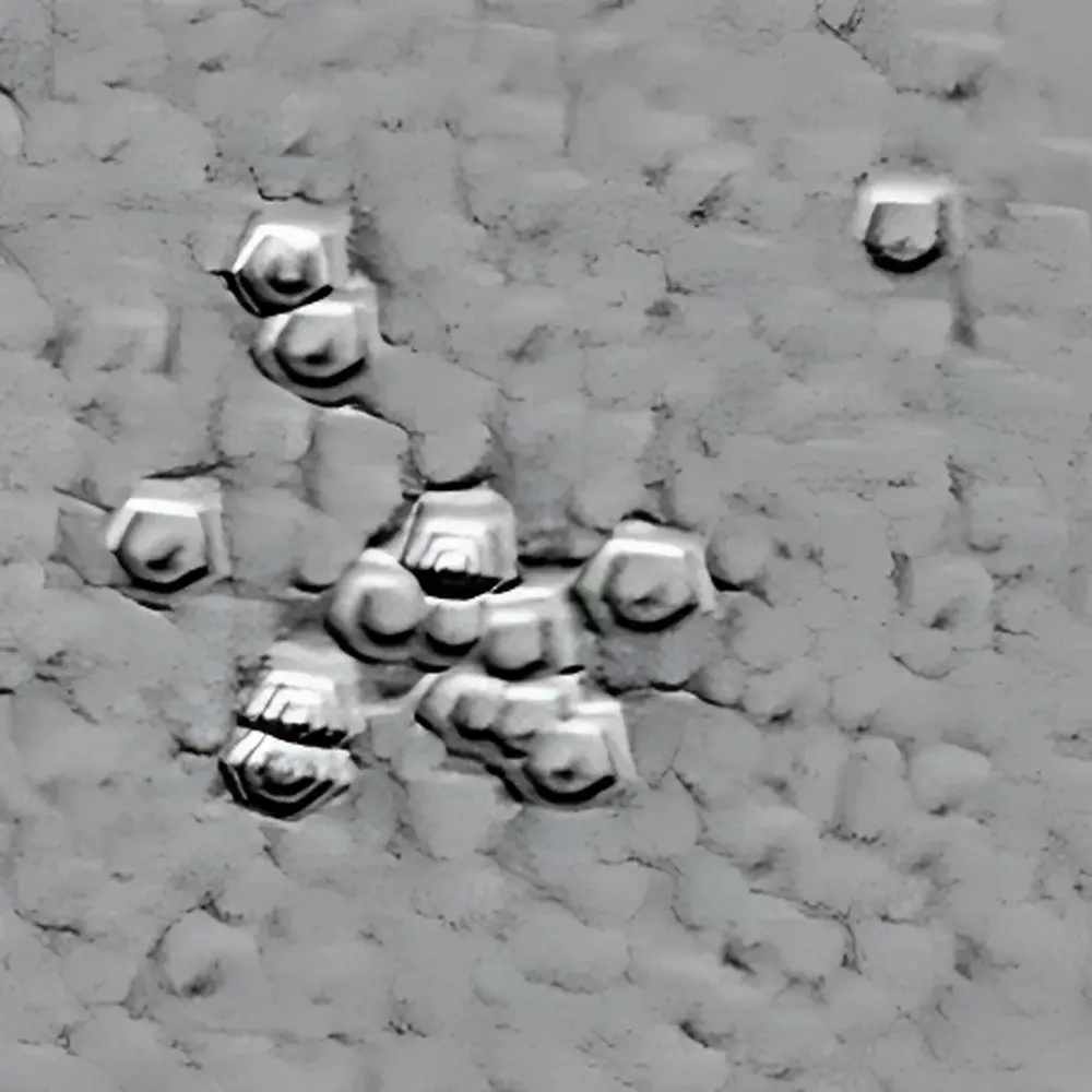
The KLA Candela® 8720 Optical Wafer Defect Inspection System is an engineered solution for high-sensitivity, non-contact optical defect detection on compound semiconductor wafers up to 200 mm in diameter. Built upon KLA’s proprietary multi-angle scatterometry architecture, the system captures spatially resolved intensity variations across two distinct incident angles—enabling robust differentiation between morphological anomalies (e.g., scratches, pits, bumps), optical property deviations (e.g., local reflectance loss, phase shifts), and optoelectronic signatures (e.g., photoluminescence quenching or enhancement). Unlike conventional bright-field or dark-field imagers constrained by single-angle illumination, the Candela 8720 leverages angular diversity to decouple scattering contributions from surface roughness, subsurface dislocations, and epitaxial layer nonuniformities—critical for GaN-on-sapphire, GaAs, and InP substrates used in RF power amplifiers, high-brightness LEDs, VCSELs, and photonic integrated circuits.
Key Features
- Dual-angle simultaneous scatter imaging with configurable polarization states for enhanced defect contrast and classification fidelity
- Integrated photoluminescence (PL) channel enabling defect-correlated carrier recombination analysis without sample contact or electrical bias
- Automated SPC-ready inspection workflow supporting real-time yield trending, binning, and process excursion alerts via standardized SECS/GEM interface
- Adaptive focus and tilt compensation for wafers ranging from 100 µm to >1 mm thickness—ensuring consistent signal-to-noise across thin-film LED epiwafers and bulk substrate platforms
- Modular optical path design accommodating optional diamond scribe calibration standards, OCR-enabled wafer ID recognition, and tower light signaling for inline integration
- Factory-calibrated scatter response traceable to NIST-traceable reference standards for inter-tool correlation in multi-fab environments
Sample Compatibility & Compliance
The Candela 8720 supports native inspection of bare and patterned compound semiconductor wafers—including GaN, GaAs, InP, SiC, and AlN—with or without dielectric passivation layers. Its optical configuration accommodates both macro-defect screening (≥5 µm cracks, slip lines, wafer warpage) and micro-defect identification (sub-µm particles, quantum-well perturbations, localized strain fields). The system meets SEMI E30 (SECS/GEM) communication protocols for factory automation integration and operates within cleanroom Class 100–1000 environments. Data acquisition and storage comply with audit-ready metadata tagging per ISO/IEC 17025 requirements, and raw image archives support retrospective root-cause analysis under GLP-aligned quality systems.
Software & Data Management
Powered by KLA’s Inspector™ software suite, the Candela 8720 delivers hierarchical defect classification using supervised machine learning models trained on validated defect libraries spanning GaN LED manufacturing, RF HEMT processing, and VCSEL epitaxy. All inspection logs include timestamped tool parameters, environmental sensor readings (temperature, humidity), and full-resolution scatter/PL image stacks stored in vendor-neutral TIFF + XML metadata format. Offline analysis modules enable cross-tool defect correlation, overlay metrology alignment, and statistical confidence interval estimation for DPMO (defects per million opportunities) reporting. Optional FDA 21 CFR Part 11-compliant electronic signature and audit trail packages are available for regulated compound semiconductor fabs.
Applications
- Incoming quality control (IQC) of GaN, GaAs, and InP substrates from multiple vendors
- Post-CMP surface uniformity assessment and scratch density quantification
- Epitaxial reactor qualification through defect density mapping across wafer lots
- Correlation of substrate-level defects (e.g., threading dislocations) with downstream device performance metrics
- Process monitoring of cleaning, etch, and anneal steps in HB-LED and micro-LED production lines
- Defect-based yield modeling for AR/VR display backplanes and 5G mmWave RF front-end modules
FAQ
Does the Candela 8720 support automated defect review with SEM or AFM correlation?
Yes—the system exports coordinate-mapped defect lists compatible with KLA’s eDR™ platform and third-party review tools via GDSII-compatible coordinate formats.
Can it detect subsurface defects in GaN-on-silicon wafers?
It detects optically active subsurface features such as dislocation clusters and stacking faults when they induce measurable scatter or PL modulation; depth resolution is limited by optical penetration depth (~1–3 µm in GaN at visible/NIR wavelengths).
Is photoluminescence excitation performed with pulsed or CW lasers?
Standard configuration uses continuous-wave 405 nm and 532 nm diode lasers; optional pulsed excitation modules are available for time-resolved PL decay analysis.
What wafer handling options are supported?
Front-end robotic loading with SMIF pod or FOUP compatibility; manual load option available for R&D labs.
How is system calibration maintained over time?
Daily automated self-check using embedded scatter standards; annual traceable recalibration service includes NIST-traceable reflectance and scatter angle verification.


