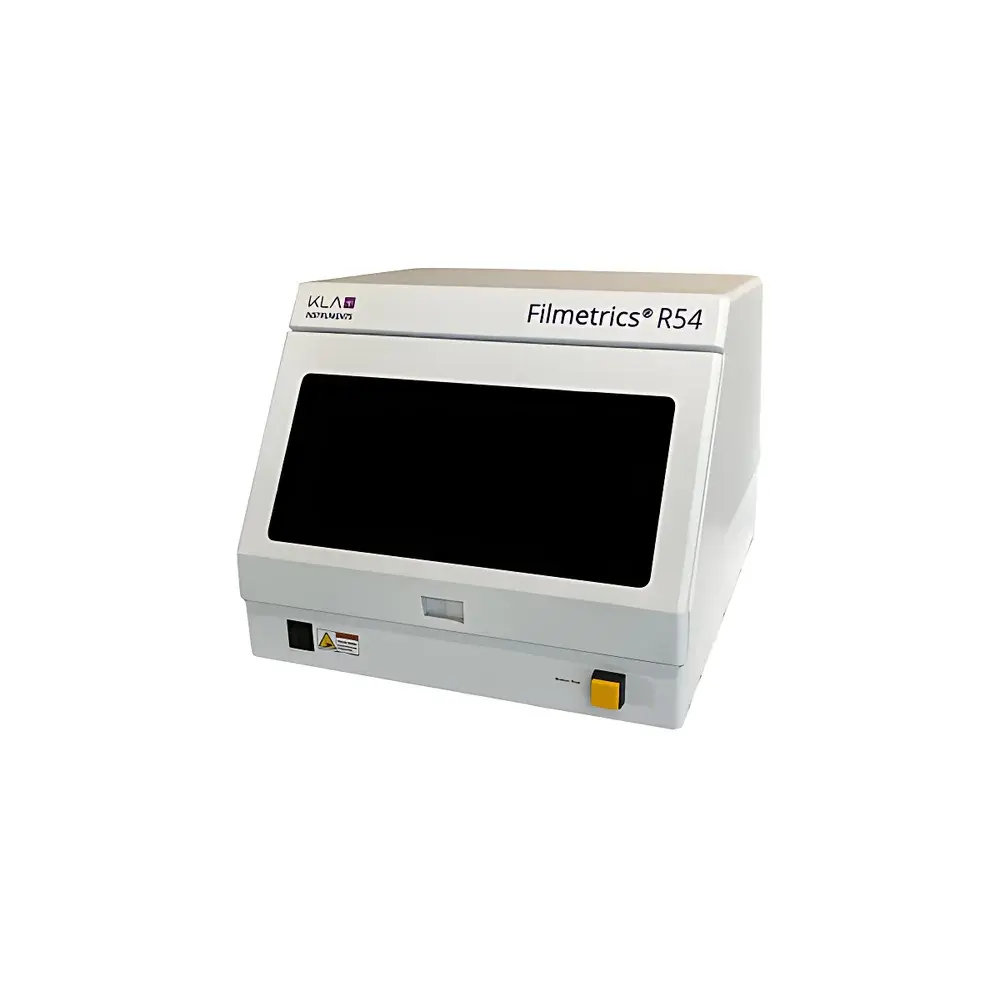
KLA R54 Four-Point Probe Sheet Resistance and Resistivity Measurement System
| Brand | KLA |
|---|---|
| Origin | USA |
| Model | R54 |
| Automation Level | Semi-Automatic |
| Resistivity Measurement Range | 1 mΩ/□ to 200 Ω/□ |
| Resistivity Measurement Accuracy | < 0.02% |
| Z-Travel Range | 15 mm |
| XY Stage Type | Motorized |
| Max Sample Height | 15 mm |
| Max Sample Weight | 2.5 kg |
| 4PP Measurement Repeatability | < 0.02% |
| EC Measurement Repeatability | < 0.2% |
| Compatible Sample Sizes | Up to 300 mm Ø or A4 (210 × 297 mm) |
| Probe Configurations | Customizable rectangular, linear, polar, and user-defined mapping patterns |
| Dual-Mode Operation | Four-Point Probe (4PP) and Non-Contact Eddy Current (EC) |
Overview
The KLA R54 Four-Point Probe Sheet Resistance and Resistivity Measurement System is a precision-engineered metrology platform designed for quantitative electrical characterization of conductive thin films in semiconductor process development and high-volume manufacturing environments. It operates on two complementary physical principles: the four-point probe (4PP) method—based on controlled current injection and voltage sensing across collinear probes—and non-contact eddy current (EC) measurement, which relies on electromagnetic induction in conductive layers. The 4PP mode is optimized for films where surface contact is permissible and thickness is less than half the probe spacing; it delivers traceable, high-reproducibility sheet resistance (Rs) data essential for process control of sputtered, evaporated, or CVD-deposited metal and doped semiconductor layers. The EC mode eliminates mechanical contact, making it ideal for soft, oxidized, or photoresist-coated surfaces—including post-lithography wafers and flexible substrates—while maintaining robust signal-to-noise performance across a 10-decade conductivity range. The R54 integrates both modalities into a single, closed-chamber architecture, enabling rapid switching between techniques without sample repositioning or environmental exposure.
Key Features
- Dual-mode operation: Seamlessly switch between four-point probe (4PP) and non-contact eddy current (EC) measurement within one platform, supporting cross-validated metrology workflows.
- Dynamic height compensation: EC probe automatically adjusts vertical position at each measurement point using real-time capacitance-based feedback, ensuring consistent lift-off distance and eliminating operator-induced variability.
- Boundary effect correction and probe spacing error compensation: Proprietary algorithms correct for edge artifacts and mechanical tolerances inherent in manual or semi-automated probe alignment, improving accuracy on small or irregularly shaped samples.
- Motorized high-precision X-Y stage with 15 mm Z-travel: Supports full-wafer mapping (up to 300 mm diameter) and A4-format flexible substrates, with positional repeatability better than ±1 µm.
- Configurable measurement layouts: Define custom scan patterns—including rectangular grids, radial sweeps, linear traverses, and user-defined coordinate lists—via intuitive software interface; up to 10,000 points per map.
- Closed-system chamber: Provides inert ambient control and light shielding, critical for photosensitive materials (e.g., organic semiconductors, photoresists) and processes requiring stable thermal or humidity conditions.
Sample Compatibility & Compliance
The R54 accommodates rigid and flexible substrates ranging from silicon and sapphire wafers to polymer foils and glass panels. Its dual-probe architecture supports characterization of metals (Al, Cu, TiN), transparent conductive oxides (ITO, AZO), doped SiGe and GaAs layers, ion-implanted silicon, and emerging materials such as graphene and conductive polymers. All measurement protocols comply with ASTM F84–22 (Standard Test Method for Measuring Resistivity of Silicon Wafers by the Four-Point Probe Method) and ISO 10474 (Metallic materials — Sheet and strip — Tensile testing). Data acquisition and reporting modules support audit-ready documentation aligned with GLP and GMP requirements, including electronic signatures, version-controlled calibration logs, and 21 CFR Part 11–compliant audit trails when integrated with enterprise-grade LIMS or MES platforms.
Software & Data Management
The R54 is operated via RSMapper™—a dedicated metrology software suite developed by KLA for thin-film resistivity analysis. RSMapper provides real-time visualization of sheet resistance, resistivity, and derived film thickness maps, with overlay capabilities for process tool matching and yield correlation. It includes built-in statistical process control (SPC) tools, Cp/Cpk calculation, and defect clustering detection based on spatial variance thresholds. Raw measurement data is stored in vendor-neutral HDF5 format, ensuring long-term archival integrity and third-party analysis compatibility (e.g., Python, MATLAB, JMP). Offline analysis mode allows post-acquisition reprocessing with updated material constants or correction models without re-measuring samples. Calibration routines are fully traceable to NIST-certified reference standards, with automated drift monitoring and recalibration alerts triggered by time or usage thresholds.
Applications
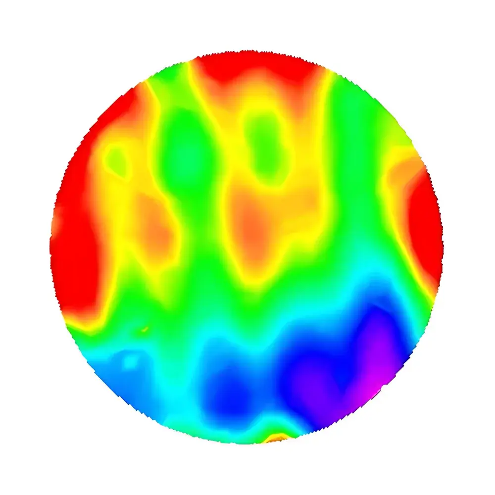
- Metal film uniformity mapping: Quantify spatial variation in Rs across sputtered Al or Cu interconnect layers to identify deposition non-uniformity, chamber wall effects, or shadowing artifacts.
- Ion implantation characterization: Monitor activation efficiency and lateral dopant distribution after rapid thermal annealing (RTA); detect “hot” or “cold” spots indicative of lamp non-uniformity or wafer-to-heater contact failure.
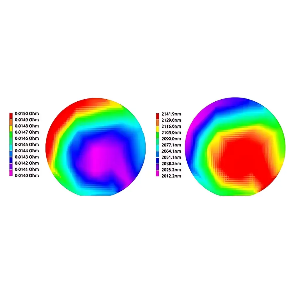
- Film thickness derivation: Using known bulk resistivity (ρ), compute thickness t = ρ / Rs; conversely, input nominal thickness to extract local resistivity variations reflecting grain structure or impurity segregation.
- Advanced packaging metrology: Characterize redistribution layer (RDL) resistivity on fan-out wafer-level packages (FOWLP), where conventional probe contact may damage fine-pitch copper traces.
- Flexible electronics QA: Perform non-destructive Rs mapping on PET- or PI-based transparent electrodes used in foldable displays and wearable biosensors.
FAQ
What is the difference between sheet resistance (Rs) and resistivity (ρ)?
Sheet resistance is an areal property expressed in ohms per square (Ω/□), independent of geometry, and is directly measured by 4PP. Resistivity is a bulk material property (Ω·cm), calculated from Rs and film thickness.
Can the R54 measure through passivation layers?
Yes—the EC mode enables measurement through dielectric capping layers (e.g., SiNx, SiO2) up to ~1 µm thick, provided the underlying conductor is sufficiently conductive.
Is probe force adjustable in 4PP mode?
Yes—mechanical probe load is programmable and calibrated to ensure consistent contact pressure across varying surface hardnesses while avoiding film damage.
Does the system support automated recipe-based measurements?
Yes—RSMapper supports saved measurement templates with predefined stage motion, probe mode selection, dwell time, and data export settings for unattended batch processing.
How often does the system require calibration?
Annual NIST-traceable calibration is recommended; however, daily verification using certified reference wafers is supported via embedded quick-check routines.


